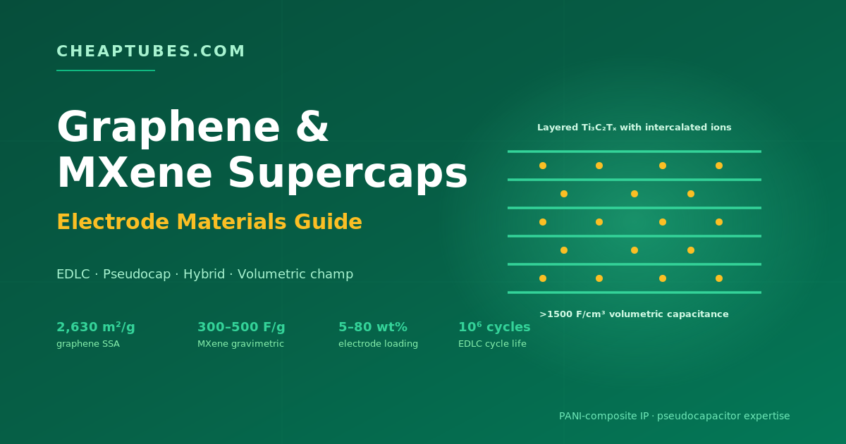
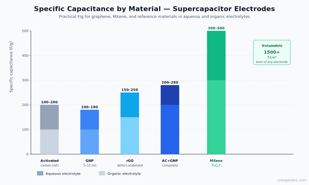
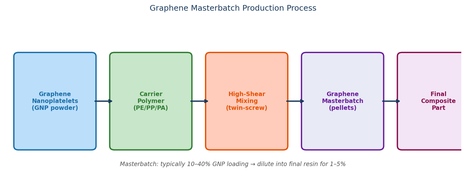
Graphene nanoplatelets, reduced graphene oxide, and MXene (Ti3C2Tx) serve as high-surface-area electrodes in electrochemical double-layer capacitors (EDLCs) and pseudocapacitors. Graphene provides up to 2,630 m²/g theoretical surface area; practical electrodes achieve 200–700 m²/g. MXene contributes both double-layer capacitance and surface-redox pseudocapacitance, achieving volumetric capacitances above 1,500 F/cm³ in optimized films — among the highest reported for any electrode material. This page covers EDLC vs pseudocapacitor selection, material-grade choice, and procurement considerations for graphene and MXene supercapacitor electrodes.
EDLC vs pseudocapacitor vs hybrid
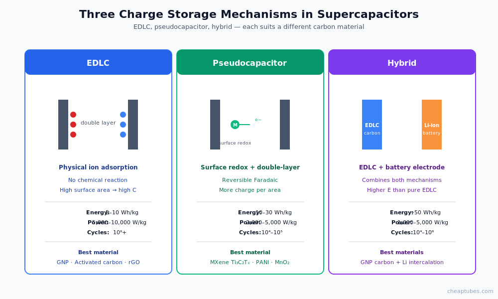
Supercapacitors store charge by three distinct mechanisms, and the right carbon material depends on which mechanism dominates:
Electrochemical double-layer capacitors (EDLCs). Charge is stored physically at the electrode-electrolyte interface — no chemical reaction, just ion adsorption on a high-surface-area substrate. Energy density is modest (5–10 Wh/kg) but power density is very high (5,000–10,000 W/kg) and cycle life is essentially unlimited (106+ cycles). EDLCs use porous carbon, activated carbon, graphene, or rGO as the electrode material.
Pseudocapacitors. Charge is stored via fast, reversible surface redox reactions in addition to double-layer adsorption. Energy density is higher than EDLCs (10–30 Wh/kg) at moderate cost in cycle life (104–105 cycles). Common pseudocapacitive materials: MnO2, RuO2, conductive polymers, and (notably) MXene Ti3C2Tx.
Hybrid supercapacitors. Combine an EDLC electrode (carbon, high power) with a battery-like electrode (lithium intercalation material, high energy). Energy density approaches 50 Wh/kg with power density retained at 1,000–5,000 W/kg. Hybrid devices increasingly dominate commercial supercapacitor product launches in 2024–2026.
The trade-offs determine material choice. For pure EDLC: maximize surface area and conductivity. For pseudocapacitor: choose a material with reversible surface redox at the operating voltage. For hybrid: carbon electrode is typically graphene-based; battery electrode follows lithium-ion design.
Three supercapacitor mechanisms – EDLC, pseudocapacitor, and hybrid – each suits a different carbon material grade.
Why surface area and conductivity = supercap performance
Specific capacitance (F/g) at the EDLC electrode is proportional to electrochemically accessible surface area times the dielectric capacitance of the electrolyte double layer. Practical EDLC carbons deliver 100–250 F/g in aqueous electrolyte and 80–200 F/g in organic electrolyte. Graphene and rGO can exceed 300 F/g in optimized configurations.
Two surface-area caveats matter:
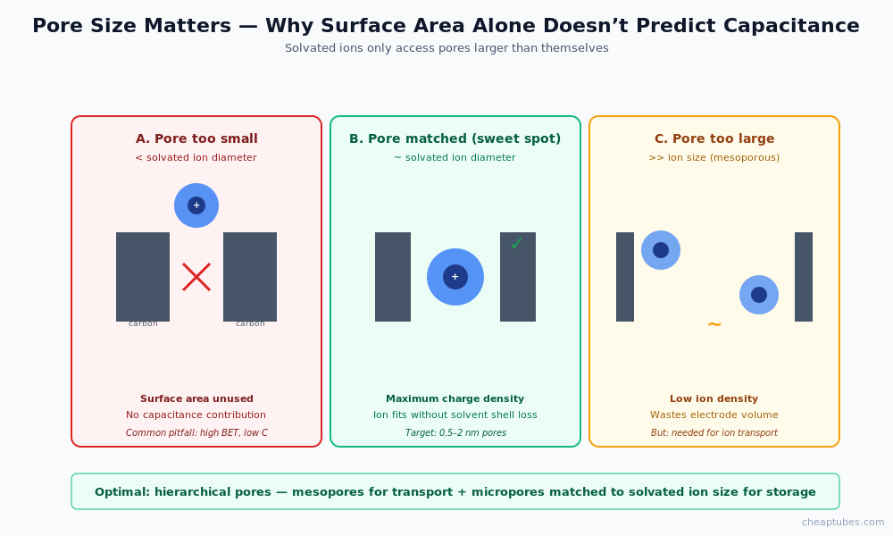
Pore size matters more than total surface area. Pores smaller than the solvated ion (1–2 nm for organic electrolytes, 0.5–1 nm for aqueous) contribute little to capacitance because ions cannot access them. Optimal carbon electrodes have a hierarchical pore structure: meso-pores for ion transport plus narrow micro-pores tuned to the solvated ion size for high-density adsorption.
Conductivity sets the rate ceiling. A high-surface-area carbon with poor conductivity delivers excellent low-rate capacitance but cannot maintain it at high rates. Graphene and MXene have intrinsic in-plane conductivities orders of magnitude higher than activated carbon, which is the reason they dominate high-power supercapacitor research.
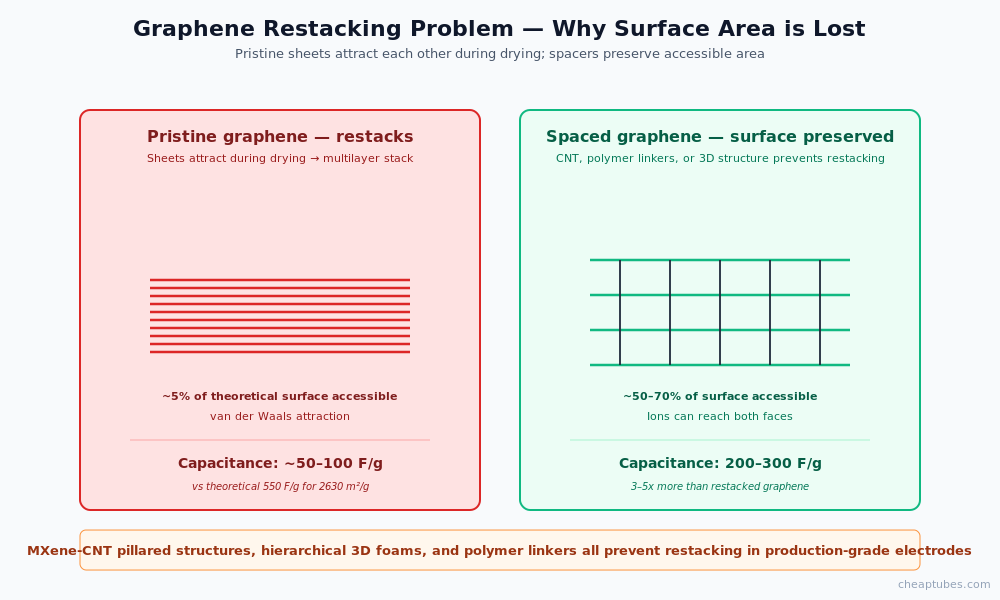
For graphene specifically, the practical challenge is that graphene sheets restack into multilayer assemblies during electrode fabrication — losing most of the theoretical surface area. Successful graphene supercapacitor electrodes use spacers (curved sheets, nanotube intercalation, polymer linkers) to prevent restacking and maintain accessible surface area.
Pristine graphene restacks during drying losing surface area – CNT spacers, polymer linkers, or 3D structures preserve accessibility.
Material-by-material breakdown
Graphene nanoplatelets (GNP) and few-layer graphene. Conductive backbone for EDLC electrodes. Practical specific capacitances 120–200 F/g in aqueous electrolyte at moderate rates. Lower capacitance than activated carbon at low rates, but far higher rate capability and far better cycle stability. Common pairing: GNP + activated carbon hybrid composite, which combines GNP’s conductivity with activated carbon’s surface area. Available from Cheap Tubes’ GNP catalog.
Graphene oxide (GO). Used primarily as a precursor for reduced graphene oxide electrodes. GO itself is electrically insulating because of the oxygen functional groups; it must be reduced to rGO before use as a supercap electrode. GO’s solubility in water and aqueous binders makes it the easiest graphene-family material to process at scale. Available via Cheap Tubes’ GO catalog.
Reduced graphene oxide (rGO). Conductivity restored, defect density tunable via reduction conditions. Practical capacitances 150–250 F/g. rGO defects are sometimes beneficial — they introduce pseudocapacitive contributions from residual oxygen groups, raising total capacitance. rGO is the most common graphene-family electrode in published supercapacitor work.
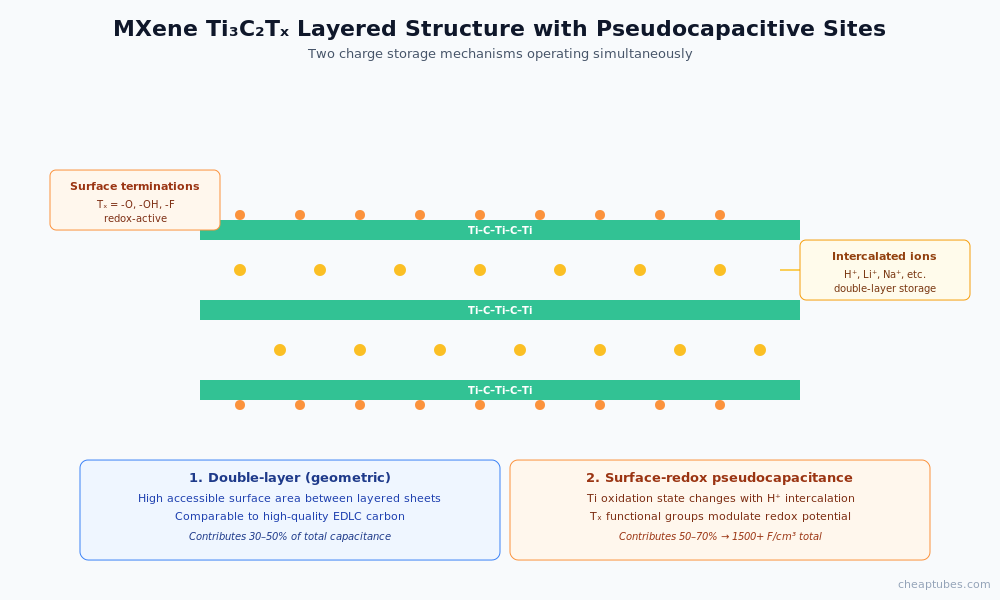
MXene Ti3C2Tx. The standout 2D material for pseudocapacitors. Layered structure with intercalated water and surface-terminating groups (-O, -OH, -F denoted Tx) that participate in reversible surface redox. Volumetric capacitances exceed 1,500 F/cm³ in dense films — among the highest reported for any electrode material. Areal capacitances of 1–2 F/cm² in thick coatings. Limitations: oxidative degradation in ambient air over long storage; performance dependent on synthesis-induced surface chemistry. Available via Cheap Tubes’ MXene category.
Composite electrodes. Most published high-performance supercap electrodes combine two or more carbon morphologies — for example, GNP backbones interleaved with activated carbon spacers, or MXene + CNT pillared structures that prevent MXene restacking. Hybrid electrodes are the current state-of-the-art for commercial-grade performance.
MXene Ti3C2Tx delivers two simultaneous charge storage mechanisms: double-layer capacitance plus surface redox pseudocapacitance.
Pseudocapacitive contributions of MXene
MXene’s high volumetric capacitance comes from two simultaneous mechanisms:
Double-layer capacitance from the high accessible surface area between layered Ti3C2Tx sheets — comparable to a high-quality EDLC carbon.
Surface-redox pseudocapacitance from oxidation-state changes of surface Ti atoms in the presence of protons or other cations. The functional groups (-O, -OH, -F) on the MXene surface modulate the redox potential and the available redox capacity. This is the contribution that distinguishes MXene from a pure-EDLC graphene electrode.
The combined effect is volumetric capacitance several times that of activated carbon or pristine graphene, with rate capability that scales with the in-plane MXene conductivity. The technology trade-offs: MXene cost is higher than graphene-family materials, and ambient-air stability is more limited (storage and processing require inert or controlled atmospheres for the highest-quality grades).
For supercapacitor R&D and commercial development teams evaluating MXene, the practical specifications to check are: Ti3C2Tx layer count (mono vs few-layer), surface termination distribution (-O, -OH, -F ratio), and pre-intercalation state (delaminated vs multilayer).
Pore size matching determines real capacitance – pores must accept the solvated ion without excluding it.
Loading in the final electrode is typically 70–95 wt% active carbon material, 5–15 wt% binder (PTFE or PVDF), 0–10 wt% conductive additive (carbon black or CNT). For composite electrodes, mass ratios of the carbon components are typically optimized empirically.
MXene Ti3C2Tx delivers 300-500 F/g gravimetric and 1500+ F/cm³ volumetric capacitance – 2-5x better than graphene-only electrodes.
For pilot or production-scale electrode coating, dispersion uniformity again drives yield. Surfactant-stabilized Flexiphene formulations are well-suited to graphene and rGO supercapacitor electrode coatings where standard NMP-based dispersion would otherwise re-bundle.
Polyaniline and polymer-composite electrodes. A growing fraction of pseudocapacitor electrode formulations combine MXene or graphene with conductive polymers — particularly polyaniline (PANI) — that contribute both pseudocapacitance and mechanical robustness. CTI Materials holds patent coverage (U.S. Patents 10,049,783 and 11,961,630) on CNT + graphene/GO/GNP composites with polyaniline, polyaminotriazole, polyimide, polyamide, nylon, and polyester polymer matrices. For supercapacitor R&D and production buyers integrating conductive-polymer composites, the Flexiphene patented dispersion technology provides validated formulations covering these exact polymer-nanocarbon chemistries.
Cheaptubes products for supercapacitor applications
Graphene Nanoplatelets — multiple lateral sizes and thicknesses for EDLC and hybrid electrodes
Simon, P. & Gogotsi, Y. — perspectives on supercapacitors (2020) (Nature Materials)
Comprehensive review — electrochemical energy storage applications of graphene oxide including supercapacitors (2024) (Energy & Fuels)
(External links reflect representative peer-reviewed literature; no endorsement implied.)
Frequently asked questions
Graphene or MXene — which is better for supercapacitors?
It depends on the metric. For gravimetric capacitance and cost, graphene-family materials (GNP, rGO) lead. For volumetric capacitance and pseudocapacitive contribution, MXene Ti3C2Tx is best-in-class. For commercial production, graphene-based EDLCs dominate by cost; MXene leads in volumetric energy density for R&D and emerging applications.
Why doesn’t pristine graphene match its theoretical capacitance?
Restacking. Graphene sheets attract each other strongly during electrode drying — multi-layer assemblies form that lose most of the theoretical surface area. Successful electrodes use spacers (CNT intercalation, polymer linkers, hierarchical structures) to keep sheets separated and surface area accessible.
Can MXene be used in aqueous and organic electrolytes?
Yes to both, with different performance characteristics. Aqueous electrolytes deliver the highest pseudocapacitive contribution (proton-mediated surface redox). Organic electrolytes enable higher operating voltage windows but reduce pseudocapacitance. Ionic-liquid electrolytes are increasingly used for high-voltage MXene cells.
How stable is MXene in ambient air?
Pristine Ti3C2Tx MXene degrades over weeks-to-months in ambient air, particularly in humid conditions. Storage under inert atmosphere or in solvent dispersions slows degradation. Surface-functionalized MXene variants and protective coatings are active development areas for improving shelf life.
What’s the role of carbon black in supercap electrodes?
In most commercial supercapacitor electrodes, the active carbon (activated carbon, graphene, rGO) provides most of the capacitance, and 5–15 wt% carbon black is added for electrical connectivity to the current collector. Replacing carbon black with CNT or graphene in the conductive-additive role can reduce loading while improving rate capability — same percolation argument as in lithium-ion cathodes.
Mike Foley is the founder of Cheap Tubes Inc. and CTI Materials LLC. He holds 2 granted U.S. patents (10,049,783 and 11,961,630) in carbon nanomaterial applications, with additional patents in prosecution. His patented materials were selected by NASA for the Enceladus mission as a dual-capacitance layer in ion-selective electrodes. Mike has supplied carbon nanomaterials to battery R&D and production for 21 years.
By Mike Foley, Founder, Cheap Tubes Inc. · Last reviewed: May 4, 2026
TL;DR
What they are — Multi-walled carbon nanotubes are concentric carbon cylinders — typically 5 to 30 walls — with outer diameters from 8 to 50 nm and lengths from 1 to 50 micrometers. Each wall is a continuous cylinder of carbon atoms (often visualized as a rolled graphene sheet, though the structure is a true tubular carbon allotrope, not a literal rolled sheet).
Why they matter — MWCNTs deliver 80-90% of the property advantages of single-walled CNTs at 10× to 100× lower cost, are available in tonnage quantities, and are the dominant carbon nanotube grade in commercial applications.
Standard purity is 98% for research-grade MWCNT. Graphitized MWCNTs reach 99.9% with markedly improved crystallinity, but the graphitization process reduces specific surface area (BET SSA) by approximately 50%.
Cheap Tubes supplies MWCNTs in research-scale grams to industrial-scale tonnage, with 7 standard diameter grades, 6 short-cut variants, 5 graphitized grades, COOH/OH/NH2 functionalized chemistries, and 5 polymer masterbatch formulations.
<!– FIGURE 1: MWCNT structure cross-section vs SWCNT side-by-side –>
Figure 1. Cross-sectional comparison of single-walled (SWCNT) and multi-walled carbon nanotube (MWCNT) structure. The MWCNT consists of multiple concentric carbon cylinders nested inside one another with characteristic 0.34 nm interlayer spacing – the same as the interlayer spacing in graphite.
What are multi-walled carbon nanotubes?
A multi-walled carbon nanotube (MWCNT) is a hollow cylindrical carbon structure made of multiple concentric tubes nested like the rings of a tree. Each wall is a continuous cylinder of sp²-bonded carbon atoms — often visualized as a rolled graphene sheet, though the structure is a true tubular carbon allotrope rather than a literal rolled sheet. Adjacent walls are spaced approximately 0.34 nm apart, the same as the interlayer spacing in graphite. A typical MWCNT has between 5 and 30 walls, an outer diameter of 8 to 50 nanometers, an inner hollow channel of 3 to 10 nm, and a length ranging from a few hundred nanometers up to 50 micrometers.
This concentric architecture is what distinguishes MWCNTs from single-walled carbon nanotubes (SWCNTs), which consist of a single carbon cylinder. MWCNTs were first observed by Sumio Iijima in 1991 — predating the widely cited SWCNT discovery — and have been the workhorse of commercial carbon nanotube applications ever since. They are easier to synthesize at scale, less expensive per gram, and far easier to handle and disperse than SWCNTs, while still delivering most of the electrical, mechanical, and thermal property advantages that make carbon nanotubes interesting in the first place.
Industrially, MWCNTs are produced almost exclusively by chemical vapor deposition (CVD), in which a hydrocarbon feedstock (ethylene, methane, acetylene, or xylene) is decomposed at 600-1000 °C over a metal catalyst (typically iron, cobalt, nickel, or molybdenum). The catalyst nanoparticles seed the growth of the tubes, with the tube diameter strongly influenced by the catalyst particle size. CVD scales well — modern fluidized-bed CVD reactors produce MWCNTs at hundreds of tonnes per year — which is the main reason MWCNTs cost a fraction of what SWCNTs do.
The properties that make MWCNTs valuable in applications come from the sp² carbon-carbon bonding within each wall. Tensile strength of an individual tube is in the range of 60 to 150 GPa (an order of magnitude higher than steel), Young’s modulus is 0.3 to 1 TPa, electrical conductivity is on the order of 100 to 1,000 S/cm along the tube axis, and thermal conductivity can exceed 3,000 W/m·K. In bulk material, the practical performance you actually achieve depends heavily on dispersion quality, alignment, and the matrix in which the tubes are embedded. <!– FIGURE 2: MWCNT morphology types — Russian doll, bamboo, telescoped –>
Figure 2. Common multi-walled carbon nanotube morphology variants. Russian-doll structure (concentric continuous walls) is the standard commercial MWCNT. Bamboo morphology has internal graphitic caps that compartmentalize the tube. Telescoped MWCNTs allow inner walls to slide axially within outer walls and are used in nanomechanical research.
MWCNT structural variations: morphology and chirality
While the textbook MWCNT is a set of perfect concentric cylinders nested inside each other — the so-called “Russian doll” structure — real MWCNTs come in several distinct morphologies. The morphology is set during CVD growth by the catalyst chemistry, growth temperature, and feedstock composition, and it has direct consequences for the properties and application fit of the resulting material.
Russian doll (concentric): The textbook MWCNT — a series of continuous, smooth-walled cylinders sharing a common axis, each wall a complete carbon cylinder. This is the most common commercial morphology, the structure produced by the Cheap Tubes standard MWCNT line, and the morphology that delivers the best mechanical, electrical, and thermal properties per gram. When most papers refer to “MWCNTs,” they mean Russian-doll tubes.
Bamboo (segmented): Tubes with internal graphitic caps that divide the inner volume into compartments, like the nodes in a bamboo stalk. Bamboo morphology arises from specific catalyst conditions (Fe-Co or Fe-Ni catalysts at moderate temperatures) and tends to have more surface defects and higher chemical reactivity than Russian-doll tubes. Useful for drug delivery (the internal compartments can host molecules), for catalyst supports where defect sites improve catalyst anchoring, and for applications that benefit from increased surface area at the expense of structural perfection.
Telescoped: A configuration where inner walls can slide axially within outer walls like a telescope. Telescoped MWCNTs are used in nanomechanical research — low-friction nanoscale bearings, oscillator structures, controlled-pull-out experiments — but are not commercially produced as a bulk material.
Herringbone and stacked-cup: Variants where the carbon layers are tilted relative to the tube axis (herringbone) or stacked perpendicular to the axis like a stack of cups (stacked-cup). These are technically “carbon nanofibers” rather than true MWCNTs, with intermediate properties between MWCNT and graphite. They are sometimes sold as MWCNTs by less rigorous suppliers, but the property differences matter — they have lower axial conductivity, lower mechanical strength, and higher chemical reactivity than concentric MWCNTs. The Cheap Tubes MWCNT line does not include herringbone or stacked-cup material.
Helical (coiled): A specialty morphology in which the tube grows in a helical or spring-like geometry rather than straight. Helical MWCNTs have unique mechanical (high toughness, spring-like compliance) and electromagnetic properties (broadband absorption from the chiral geometry). The Helical Multi Walled Carbon Nanotubes product is the Cheap Tubes specialty grade for these applications.
On chirality: Each individual wall of an MWCNT has its own chirality, defined by the (n,m) chiral indices that determine whether that wall is metallic or semiconducting. For SWCNTs, this matters enormously — chirality controls bandgap, optical absorption, and electronic transport. For MWCNTs, the situation is fundamentally different: each wall has its own chirality, the chiralities of adjacent walls are statistically uncorrelated, and a typical MWCNT therefore contains a mix of metallic and semiconducting walls (~1/3 metallic, 2/3 semiconducting on average). The bulk MWCNT material behaves semi-metallically. Unlike SWCNTs, MWCNTs cannot be separated by chirality, and chirality-specific electronic properties are washed out by multi-wall averaging.
Why choose MWCNTs over SWCNTs?
Single-walled carbon nanotubes have higher per-tube performance numbers — higher specific surface area, higher electrical conductivity per gram, higher mechanical reinforcement efficiency. But the gap between SWCNT and MWCNT performance in real applications is much smaller than the price gap between them. SWCNTs typically cost $50 to $500 per gram for research-grade material; MWCNTs cost $0.10 to $5 per gram for industrial grades and $5 to $50 per gram for research-grade.
For most commercial applications — conductive composites, battery additives, EMI shielding, antistatic coatings — MWCNTs deliver 80 to 90% of the property benefit at 10 to 100 times lower cost. That is why most commercially deployed CNT-enabled products on the market today (lithium-ion batteries with CNT conductive additives, conductive plastics for ESD applications, EMI shielding compounds, certain reinforced elastomers) use MWCNTs as the workhorse material.
SWCNTs are used where performance specifically demands them — high-sensitivity sensors, biomedical applications, transparent conductive films with extreme transparency-to-conductivity ratios, single-tube electronic devices, and certain polymer composite and film applications where the unique single-wall architecture delivers properties that MWCNTs cannot match. (Cheap Tubes founder Mike Foley holds granted patents on SWCNTs in polymer and film applications.) These markets are smaller in volume but commercially important.
The MWCNT advantage is not just price. MWCNTs are also dramatically easier to work with in real production environments. SWCNTs bundle together with extreme van der Waals attraction and require harsh dispersion conditions (high-power sonication, aggressive surfactants) to break apart. MWCNTs disperse more readily, especially at the larger diameters (20-50 nm), and tolerate standard dispersion equipment found in any composites lab or coatings line.
Choose SWCNTs when you specifically need single-wall electronic properties (semiconducting/metallic distinction, transparent conductors, single-tube transistors), maximum surface area per gram (catalysis, sensing), or high-performance polymer/film applications where SWCNT geometry delivers properties MWCNTs cannot. Choose MWCNTs for the broad middle of carbon-nanotube-enabled applications where cost-to-performance ratio is the dominant consideration. <!– FIGURE 3: Diameter range visualization — 8nm to 50nm with relative scale and typical applications –>
Figure 3. Cheap Tubes MWCNT diameter range from 8 nm to 50 nm, shown to relative scale in cross-section. Smaller-diameter MWCNTs deliver higher BET specific surface area and higher aspect ratio per gram; larger-diameter tubes disperse more easily and offer better cost-per-kilogram for bulk industrial applications.
Decision 1: Outer Diameter
Outer diameter is the most consequential single specification when choosing an MWCNT grade. It influences nearly every other property of the material in a predictable way.
Smaller diameters (8 to 15 nm) have higher specific surface area (typically 200-300 m²/g), higher aspect ratio per unit weight, and more efficient mechanical reinforcement at low loadings. They are the standard choice for lithium-ion battery additives where the tube must wrap around active particles, for high-performance conductive composites where electrical percolation should be reached at the lowest possible loading, and for biomedical applications where surface chemistry matters more than bulk volume. Cheap Tubes offers Multi Walled Carbon Nanotubes 8 nm and Multi Walled Carbon Nanotubes 8-15 nm for these applications.
Mid-range diameters (10 to 30 nm) are the workhorse of commercial composite applications. They provide a strong balance of surface area, reinforcement efficiency, dispersion ease, and cost. The Multi Walled Carbon Nanotubes 10-20 nm and Multi Walled Carbon Nanotubes 20-30 nm grades are the most-shipped MWCNT diameters across our industrial customer base, used in conductive polymer composites, EMI shielding compounds, and antistatic coatings.
Larger diameters (30 to 50 nm) trade per-tube performance for bulk economics, dispersion ease, and process robustness. With outer diameters in this range, BET surface area drops to 50-150 m²/g, but the tubes are easier to wet out, mix into resins without specialized equipment, and produce at high tonnage. These grades — Multi Walled Carbon Nanotubes 30-50 nm and Multi Walled Carbon Nanotubes 50 nm — are the right call for high-volume conductive plastics, tire reinforcement, structural composites where cost-per-kilogram matters, and any application where you are buying MWCNTs by the drum rather than the kilogram.
The general principle: smaller diameter buys you more property per gram but at higher cost and harder dispersion. Larger diameter buys you more bulk volume per dollar with easier processing.
Decision 2: Length — Standard vs Short Cuts
Cheap Tubes offers MWCNTs in two length classes: standard length (typically 5 to 50 micrometers, depending on grade) and short cuts (typically 1 to 2 micrometers).
Standard-length MWCNTs maximize aspect ratio (length-to-diameter ratio), which is the dominant factor in mechanical reinforcement efficiency and electrical percolation threshold. Higher aspect ratio means you reach the conductive percolation network at a lower CNT loading, which directly reduces cost in a conductive composite. Standard length is the default choice for conductive composites, EMI shielding, polymer reinforcement, and most industrial applications.
Short-cut MWCNTs are mechanically chopped to shorter lengths through controlled milling or acid treatment. The tradeoff: lower aspect ratio means higher loading is needed to reach percolation, but the tubes disperse far more easily, settle more slowly in suspensions, and exhibit lower viscosity in fluid systems. Short cuts are preferred for biomedical applications, ink-jet-compatible conductive inks, dispersion-critical sensor applications, transparent conductive coatings where aggregate-free tube networks matter more than long-range conductivity, and any flow-coating or printing process where rheology matters.
The Cheap Tubes Short Multi Walled Carbon Nanotubes line covers the same diameter range as standard MWCNTs (8 nm to 50 nm) plus full COOH and OH functionalized variants. If you are uncertain whether your application benefits from standard or short, the test is whether you need maximum reinforcement at low loading (use standard) or maximum dispersion stability and processability (use short).
Cheap Tubes MWCNTs are available in three purity grades, each appropriate for distinct applications.
Industrial Grade MWCNT — 95% carbon purity, optimized for cost and bulk supply. Acceptable residual catalyst metals (iron, cobalt, nickel) and amorphous carbon for applications where extreme purity is not required. The Industrial Grade MWCNT line is built for high-volume conductive composites, EMI shielding compounds, antistatic plastics, tire reinforcement, and any application where a few percent of metal residue does not affect performance and the price-per-kilogram drives the buying decision.
Standard Research-Grade MWCNT — 98% carbon purity by TGA, with low residual ash content and uniform diameter distribution. This is the typical research and development grade — appropriate for most laboratory experiments, prototype composites, and applications where moderate purity matters but extreme purity is not required. The Standard MWCNT line covers diameters from 8 nm to 50 nm at 98% purity.
Graphitized MWCNT (GMWCNT) — 99.9% carbon purity with significantly improved crystalline structure. Graphitization is a high-temperature post-treatment (typically 2,500 to 3,000 °C in inert atmosphere) that drives off residual catalyst metals, removes amorphous carbon and structural defects, and rearranges the graphene walls into a more perfect crystalline structure. The result is dramatically better electrical conductivity per tube, higher thermal conductivity, improved oxidation resistance, and better mechanical properties.
The graphitization tradeoff is real and worth understanding before buying: the graphitization process reduces BET specific surface area by approximately 50% because it closes off small pores, smooths surface defects, and consolidates the wall structure. A standard MWCNT with BET SSA of 200 m²/g typically becomes a graphitized MWCNT with 100 m²/g.
This SSA loss is desirable when you are choosing graphitized MWCNT for its electrical, thermal, or mechanical properties — the lower defect density that gives you better conductivity is exactly what reduces the surface area. But it is undesirable when you need surface area for catalyst loading, ion access in battery electrodes, or surface adsorption applications.
Choose graphitized MWCNT when: aerospace structural composites, thermal management systems, demanding electrical conductivity (transparent electrodes, supercapacitor electrodes that prioritize conductivity over capacitance), high-performance EMI shielding, and any application where defect density is the limiting factor.
Choose standard 98% MWCNT when: catalyst supports (need high SSA), battery anodes where ion access through tube networks matters more than per-tube conductivity, conductive composites where cost matters more than crystallinity, EMI shielding at moderate frequencies, and any application where the SSA loss hurts more than the crystallinity gain helps.
The Graphitized MWCNT line covers diameters from 8-15 nm to 50 nm, with COOH and OH functionalized variants available.
Decision 4: Functionalization Chemistry
Pristine MWCNTs are hydrophobic and chemically inert. Their outer wall consists of sp²-bonded carbon with no surface functional groups — the same chemical character as graphene or graphite. This works fine for many applications but limits dispersion in polar solvents, prevents covalent bonding to polymer matrices, and rules out chemistries that need surface functional groups for activation.
Functionalization adds chemical handles to the outer wall, opening up dispersion in water, covalent attachment to polymer backbones, anchoring of catalysts or biomolecules, and improved interfacial bonding in composites. Cheap Tubes offers three production functionalization chemistries:
COOH (carboxyl) functionalization is produced by oxidative treatment of the MWCNT surface, typically with concentrated nitric acid or a mixed acid system. The result is carboxylic acid groups (-COOH) attached to the outer wall, primarily at defect sites and tube ends. COOH-MWCNTs are the most widely used functionalized grade — they disperse readily in water and polar solvents, can be further modified by amidation or esterification chemistry, and bond covalently to amine-containing polymers (epoxy curing agents, polyamides). Use COOH for aqueous dispersions, water-based inks, biomedical applications, conductive composites with amine-cured epoxies, and any chemistry that needs a starting handle for further modification. The COOH-functionalized MWCNT line spans all standard diameters.
OH (hydroxyl) functionalization produces hydroxyl groups (-OH) on the outer wall through hydrogen peroxide treatment or controlled oxidation. OH-MWCNTs are slightly less polar than COOH-MWCNTs but offer different bonding chemistry — hydroxyls can hydrogen-bond to polymers, esterify with acid groups, and react with isocyanates to form urethane linkages in polyurethane composites. Use OH for polyurethane composites, esterification-based grafting, hydrogen-bonded interactions with starches or cellulose, and any system where COOH would over-acidify the matrix.
NH2 (amine) functionalization introduces primary amine groups (-NH2) to the outer wall, typically through a multi-step synthesis from COOH precursors. NH2-MWCNTs are nucleophilic and react readily with epoxies, carboxylic acids, and isocyanates. They are the right choice for epoxy composites where you want covalent bonding without an amine curing agent doing the work, for biomolecule conjugation, and for surface chemistry that needs an amine starting point. The NH2-functionalized MWCNT 20 nm is available as a standard product.
Functionalization comes with tradeoffs. The oxidative treatments that introduce COOH and OH groups also damage the outer wall structure, which reduces electrical conductivity along the tube axis (typically by 10-30%) and reduces mechanical strength. For applications where pristine electrical properties matter — supercapacitor electrodes, transparent conductors — use pristine MWCNTs and engineer dispersion through surfactants instead of covalent functionalization.
Combinations are also available: graphitized + COOH, graphitized + OH, industrial + COOH, industrial + OH, short + COOH, short + OH. The full functionalization matrix lets you pick a base grade for purity and structural quality, then add the surface chemistry you need. <!– FIGURE 4: MWCNT application landscape –>
Figure 4. Major commercial application categories for multi-walled carbon nanotubes (MWCNTs), organized by end-use industry with recommended grade and typical loading range. Conductive polymer composites and lithium-ion battery additives represent the largest MWCNT markets by volume.
MWCNT vs SWCNT vs GNP — when to use which
Choosing between MWCNT, SWCNT, and graphene nanoplatelets (GNP) is a recurring decision for anyone working with carbon nanomaterials. The materials overlap in some applications and diverge sharply in others.
Use MWCNTs when: you need carbon nanotube performance at industrial cost, you are making conductive composites or polymer masterbatches, you need tonnage supply, you are formulating lithium-ion battery additives, your application is EMI shielding or antistatic coatings, or you need a balance of electrical, mechanical, and thermal properties at a reasonable price.
Use SWCNTs when: you specifically need single-wall electronic properties (semiconducting/metallic separation, transparent conductors with extreme transparency-to-conductivity ratios), you need maximum surface area per gram for catalysis or sensing, you are working on transistor-scale electronics, you need SWCNT-specific polymer or film performance, or your budget supports the 10-100× cost premium. See our SWCNT Buying Guide for detailed selection criteria.
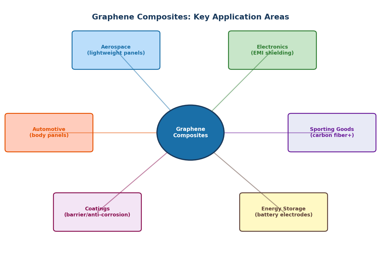
Use GNPs when: you need a 2D form factor (in-plane conductivity, planar reinforcement of films and coatings), you are making graphene-reinforced concrete or asphalt, you need anti-corrosion barrier properties, you are formulating thermal interface materials where in-plane thermal conductivity matters, or you need the cheapest carbon nanomaterial that still delivers measurable property improvements. See our GNP Buying Guide for detailed selection criteria.
The three materials are often used in combination. A high-performance battery electrode might use SWCNTs for conductive bridging between active particles, MWCNTs for the bulk conductive network, and GNPs for in-plane current collection. A high-end aerospace composite might use MWCNTs for through-thickness reinforcement and GNPs for in-plane stiffness. The materials are complementary as often as they are competitive. <!– FIGURE 5: Conductive composite percolation curve –>
Figure 5. Electrical percolation curve for an MWCNT-loaded polymer composite. Bulk resistivity drops by 8 to 12 orders of magnitude across a narrow loading range centered on the percolation threshold (~0.5 wt% for high-aspect-ratio MWCNTs with good dispersion). The threshold position and steepness depend on multi-walled carbon nanotube aspect ratio, alignment, and dispersion quality.
Application-specific recommendations
Conductive polymer composites
The largest commercial application of MWCNTs by volume. Adding MWCNTs to an insulating polymer matrix transforms it into an electrically conductive material once the loading exceeds the percolation threshold — typically 0.1 to 1 wt% for high-aspect-ratio MWCNTs, depending on dispersion quality. Above percolation, electrical resistivity drops by 8 to 12 orders of magnitude, from insulator to semiconductor or even conductor regimes.
MWCNTs are added to both cathode and anode formulations as conductive additives, replacing or supplementing carbon black at lower total loadings. The CNT network provides long-range electronic connectivity between active material particles, improving rate capability and cycle life. Cathode applications typically use 0.5 to 1.5 wt% MWCNT versus 2 to 5 wt% carbon black. Anode applications, particularly silicon-graphite composites, benefit from the mechanical buffering of CNT networks during the volume changes of silicon.
MWCNTs provide effective electromagnetic interference shielding in polymer composites at low loadings (typically 1-5 wt%) by forming a conductive network that absorbs and reflects incident electromagnetic radiation. Higher aspect ratio MWCNTs work at lower loadings; thicker tubes provide bulk volume advantages for cost-driven applications.
Recommended grade: Standard 98% MWCNT with high aspect ratio (10-30 nm diameter, standard length) for low-loading EMI shielding. For higher-frequency shielding (5 GHz and above), graphitized MWCNT improves performance by reducing dielectric losses. Best products: Multi Walled Carbon Nanotubes 10-20 nm, Graphitized Multi Walled Carbon Nanotubes 10-20 nm.
Antistatic and ESD coatings
For applications that need surface resistivity in the 10⁵ to 10¹² ohm/square range — electronics packaging, cleanroom flooring, fuel handling — MWCNTs provide controlled, stable, low-loading conductivity that does not degrade with aging or humidity (unlike conductive carbon black or metal flake systems). Loading levels of 0.5 to 2 wt% are typical.
Carbon-fiber-reinforced polymer (CFRP) composites in aerospace applications benefit from MWCNT additions to the matrix resin, which improves through-thickness conductivity (for lightning strike protection), interlaminar shear strength, fatigue resistance, and damage tolerance. Aerospace applications demand the highest available material quality.
MWCNT-loaded polymer composites and thermal interface materials (TIMs) leverage the high axial thermal conductivity of CNTs (3,000+ W/m·K per tube) to improve heat transfer in electronics packaging, LED lighting, and battery thermal management systems. The bulk thermal conductivity improvement depends strongly on tube alignment and interfacial thermal resistance.
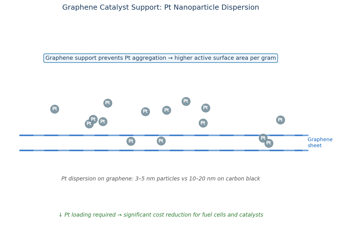
MWCNTs are used as catalyst supports in fuel cells, hydrogen evolution reactions, hydrogenation, and oxidation chemistry. Their high surface area, chemical stability, electrical conductivity (for electrocatalysis), and tunable surface chemistry make them attractive supports for platinum, palladium, and various transition-metal nanoparticles. Catalyst applications need high BET SSA — graphitized grades are not appropriate.
Helical (coiled) MWCNTs have a unique spring-like morphology with mechanical and electromagnetic properties that differ from straight tubes. They are used in mechanical sensors (strain gauges with high gauge factor), broadband EMI absorption, and specialized composite applications where their helical geometry improves toughness or damping. The Helical Multi Walled Carbon Nanotubes product is a specialty grade for research applications.
Polymer masterbatches — the industrial shortcut
For commercial production, mixing dry MWCNT powder directly into a polymer is technically possible but rarely optimal. The MWCNT powder has very low bulk density (0.05-0.15 g/cm³), tends to bridge in feeders, generates dust during handling, and requires significant compounding energy to achieve good dispersion in the matrix.
A polymer masterbatch — MWCNT pre-dispersed at high loading (typically 10-20 wt%) into a base polymer — solves all of these problems at once. Masterbatches are pelletized, easy to feed, dust-free, and already pre-dispersed using high-shear equipment optimized for the matrix polymer. The compounder then dilutes the masterbatch into the final compound at the target loading using standard extrusion or molding equipment.
Cheap Tubes offers polymer masterbatches in five standard matrix polymers covering the most common engineering plastics:
For epoxy systems, the Carbon Nanotubes Epoxy Composite provides MWCNT pre-dispersed in an epoxy resin matrix, ready for two-part formulation work.
When the production volume is more than a few kilograms of finished compound per month, masterbatches almost always win on cost-per-finished-part, dispersion quality, and process robustness. <!– FIGURE 6: Production methods comparison –>
Figure 6. MWCNT production method comparison. Chemical vapor deposition (CVD) dominates commercial production at hundreds of tonnes per year, while arc discharge and laser ablation are mostly historical or limited to specialty research applications today.
Pricing tiers and supplier categories
The MWCNT market segments into three distinct supplier categories, each appropriate for different buyer profiles.
Category A — High-volume mass producers (typically $50-500/kg)
A small number of producers operate large CVD reactors at multi-tonne annual scale, supplying primarily to battery cathode manufacturers, plastics compounders, and tire manufacturers. The economics work at hundreds of kilograms or tonnes per order, with fixed product specifications and limited customization. Quality variation between lots can be significant. Best fit: established commercial production with stable, high-volume requirements and budget for in-house QC. Not appropriate for R&D, prototyping, or applications requiring lot-to-lot consistency at small scale.
Distributors like Cheap Tubes serve the middle of the market: research-grade MWCNT with representative characterization data, multiple purity grades, broad diameter and functionalization options, and the option to scale up to industrial quantities for production. A Technical Data Sheet (TDS) with representative TGA, BET, Raman, and TEM data is provided per product. Order quantities range from gram-scale research samples to industrial drum quantities. This is the right tier for university research, pre-production R&D, and most commercial applications below the multi-tonne scale. Cheap Tubes has supplied this market for 21 years.
Category C — Boutique synthesis houses ($500-5,000/g)
Specialty providers offering custom MWCNT synthesis — specific length distributions, novel functionalizations, isotopically labeled tubes, alignments and arrays, peer-reviewed sample-grade material for high-impact publications. Rare-earth pricing, weeks to months of lead time. Appropriate for top-tier academic groups doing fundamental physics or chemistry research where the experimental design demands a specific, exotic specification not available off the shelf.
The pricing within each category varies by purity grade, functionalization, diameter, length, and order volume. As a rough guide for Category B research-grade Cheap Tubes pricing: industrial-grade pristine MWCNT runs $2-15 per gram, standard 98% pristine runs $5-30 per gram, graphitized runs $20-80 per gram, and functionalized variants add 50-100% to the base price. Bulk discounts apply at kilogram and 10-kilogram scales.
Dispersion guidance
Achieving good MWCNT dispersion is the single biggest factor between a composite that delivers the predicted property improvement and one that fails. Aggregated MWCNT powder behaves like a filler — it adds weight without adding the properties you bought it for. Properly dispersed MWCNTs, distributed as individual tubes or small bundles throughout the matrix, deliver the conductive network, mechanical reinforcement, and thermal pathways that drive every CNT-enabled application.
For aqueous dispersions: Use COOH or OH functionalized MWCNT at 1-5 mg/mL with a surfactant (sodium dodecylbenzenesulfonate at 0.5 wt%, sodium cholate at 1 wt%, polyvinylpyrrolidone (PVP) at 0.5-2 wt%, or Triton X-100 at 0.5 wt%) and probe-tip sonication in a water-cooled vessel for 30-60 minutes total active time. PVP is particularly useful for biomedical and electrode applications where downstream chemistry is incompatible with anionic surfactants.
Sonication best practices to preserve tube length and avoid heat-induced re-aggregation:
Keep amplitude below 30%. Higher amplitudes will fragment MWCNTs by sonochemical scission, reducing aspect ratio and degrading the property advantages you bought the tubes for.
Pulse the sonicator: 30 seconds on / 30 seconds off. Continuous sonication generates heat faster than the cooling bath can remove it, and the cumulative cavitation energy shortens tubes through repeated impact. Pulsed sonication preserves tube length while still delivering enough cumulative active time to achieve dispersion.
Monitor temperature at the dispersion vessel. Excessive heat re-aggregates the tubes; the surfactant becomes ineffective above its cloud point.
Use an ice bath around the vessel for any dispersion run longer than 15 minutes total active time.
For organic-solvent dispersions: N-methyl pyrrolidone (NMP), dimethylformamide (DMF), and dimethylacetamide (DMAc) are the strongest CNT solvents and disperse pristine MWCNTs without surfactants. For less aggressive solvents (acetone, ethanol, isopropanol), pre-functionalized MWCNTs (COOH for polar protic solvents, OH for protic alcohols) disperse better than pristine.
For polymer compounding: Three approaches in increasing order of dispersion quality and increasing order of capital expense. (1) Direct compounding of dry MWCNT powder into the molten polymer in a twin-screw extruder — works for simple geometries and high loadings, marginal for low-loading high-aspect-ratio applications. (2) Solution mixing — dissolve the polymer, disperse MWCNTs separately, mix and precipitate or cast — best dispersion quality but only practical for polymers that dissolve readily and for small batch sizes. (3) Masterbatch dilution — pre-dispersed MWCNT masterbatch fed alongside virgin polymer in a standard extruder, diluted to the target loading — best balance of dispersion quality and process scalability.
For epoxies and thermosets: Pre-disperse MWCNTs in the resin (Part A) using a three-roll mill or high-shear mixer at 60-80 °C, degas under vacuum, then add the curing agent (Part B) and complete the cure cycle. The pre-dispersed Carbon Nanotubes Epoxy Composite skips the dispersion step entirely and is ready for two-part formulation. <!– FIGURE 7: Purity-grade-vs-price scatter –>
Figure 7. Cheap Tubes MWCNT product line organized by carbon purity grade (95% industrial, 98% standard, 99.9% graphitized) versus typical research-scale price per gram. Each tier serves distinct application requirements, with graphitized MWCNT trading approximately 50% reduced BET surface area for substantially improved crystallinity and structural quality.
Quality and QC indicators on the TDS
A reputable MWCNT supplier provides a Technical Data Sheet (TDS) for each product with the representative technical specifications that matter for the application. The four most important specifications and how to interpret them:
Carbon purity by TGA (thermogravimetric analysis) — measured by burning the sample in air and reporting residual ash as a percentage. Industrial grade (95% pure) typically shows 3-5% residual ash (residual catalyst metals); standard 98% grade shows 1-2%; graphitized 99.9% grade shows 0.1% or less. The TGA also reveals oxidation onset temperature, which correlates with structural quality — higher onset means more crystalline, fewer defects.
BET specific surface area (SSA) — measured by nitrogen adsorption at 77 K, reported in m²/g. For MWCNTs, the BET SSA depends on tube diameter (smaller tubes = higher SSA), wall count (fewer walls = higher SSA per gram), and graphitization state. Representative values: standard 8-nm MWCNT 250-300 m²/g, standard 20-30 nm MWCNT 150-200 m²/g, standard 50 nm MWCNT 50-100 m²/g, graphitized variants approximately half these values.
Raman D/G ratio — measures the relative intensity of the disorder-related D band (around 1,350 cm⁻¹) versus the graphitic G band (around 1,580 cm⁻¹). Lower D/G ratio means fewer structural defects and higher crystallinity. Standard MWCNT typically shows D/G in the range of 0.8 to 1.5; graphitized MWCNT typically shows 0.1 to 0.5. A representative Raman spectrum should be reported on the TDS along with the D/G value.
TEM (transmission electron microscopy) characterization — confirms the diameter distribution, wall count, and morphology of the tubes. A reputable TDS includes representative TEM images showing the tube architecture. Diameter distribution should be tight (narrow distribution around the nominal diameter); wall counts should be consistent with the specification.
If a supplier cannot provide TGA, BET, Raman, and TEM data on the product TDS, treat that as a quality red flag. Application performance depends directly on these properties, and supplier transparency about characterization methodology is the strongest quality signal in the CNT market.
Bulk and tonnage supply capability
Cheap Tubes can supply MWCNTs in quantities ranging from research-scale 1-gram samples up to industrial tonnage. For bulk orders (10 kg and above), the standard product line is available at volume pricing, with discounts that scale with order size. For tonnage requirements (1,000 kg and above), we work directly with the buyer to confirm specifications, lock in lot-to-lot consistency, and arrange logistics for industrial freight.
The MWCNT product line that scales most readily to bulk volume is the Industrial Grade family — the 10 nm, 10-30 nm, and 20-40 nm industrial grades, plus their COOH and OH functionalized variants — are designed for high-volume commercial production with consistent specifications across large lots.
Standard 98% research-grade MWCNTs scale to kilogram and 10-kilogram quantities with tight product specifications and representative TDS data. Graphitized MWCNTs are available at the kilogram scale; tonnage quantities of graphitized material require lead time of 4-8 weeks.
For commercial battery, composite, masterbatch, and EMI shielding applications scaling to production volume, contact us to discuss specifications, pricing, and logistics. We have supplied this market for 21 years and have established relationships across the full MWCNT supply chain.
About the author
Mike Foley is the founder of Cheap Tubes Inc. and CTI Materials LLC, with 21 years of experience in carbon nanomaterials supply and a prior background in semiconductor wafer fabrication and thin film optics manufacturing dating to 1994. Mike holds 2 granted U.S. patents in carbon nanomaterial applications, and his patented materials were selected by NASA for the Enceladus mission as a dual-capacitance layer in ion-selective electrodes designed to detect bacterial secretions in the search for evidence of extraterrestrial life. He is based in southern Vermont.
Frequently asked questions
1. What is the difference between MWCNT and SWCNT?
A single-walled carbon nanotube (SWCNT) is a single sheet of graphene rolled into a cylinder. A multi-walled carbon nanotube (MWCNT) consists of multiple concentric SWCNT-like cylinders nested inside each other, with 5 to 30 walls being typical. SWCNTs have higher per-tube performance (higher conductivity, higher surface area, higher mechanical strength); MWCNTs are 10-100× cheaper, easier to disperse, and available in tonnage quantities.
2. What outer diameter MWCNT should I choose?
Smaller diameters (8-15 nm) deliver higher surface area, higher aspect ratio, and better mechanical reinforcement per gram, but cost more and disperse less easily. Larger diameters (30-50 nm) trade per-tube performance for bulk economics and process robustness. The most-shipped diameter range across commercial applications is 10-30 nm — a strong balance of properties, dispersion ease, and cost.
3. What is the difference between standard MWCNT and graphitized MWCNT?
Standard MWCNT has 98% carbon purity. Graphitized MWCNT has been heat-treated to 2,500-3,000 °C in inert atmosphere, removing residual catalyst metals and structural defects, reaching 99.9% carbon purity with a more crystalline structure. Graphitization improves electrical conductivity, thermal conductivity, oxidation resistance, and mechanical properties — but reduces BET specific surface area by approximately 50%. Choose graphitized for aerospace, thermal management, high-end electronics, and applications where defect density limits performance. Choose standard 98% when you need surface area, when cost matters, or when the SSA loss outweighs the crystallinity gain.
4. Should I use pristine, COOH, OH, or NH2 functionalized MWCNT?
Match the functionalization chemistry to the host matrix. Use pristine for maximum electrical conductivity per tube and for non-polar solvent or polymer systems (polyolefins, styrenics, most pristine elastomers). Use COOH for water-based dispersions, biomedical applications, and amine-cured epoxy composites. Use OH for polyurethane composites, hydrogen-bonded interactions with starches/cellulose, and esterification chemistry. Use NH2 for direct epoxy bonding and biomolecule conjugation. Functionalization reduces electrical conductivity by 10-30%, so use pristine when conductivity is the dominant requirement and the host matrix tolerates a hydrophobic filler.
5. What is the percolation threshold for MWCNT in a polymer composite?
For high-aspect-ratio MWCNTs (10-30 nm diameter, standard length) with good dispersion, electrical percolation typically occurs between 0.1 and 1 wt% loading. Poor dispersion shifts the threshold upward; lower-aspect-ratio short cuts shift it upward; smaller diameter at the same length shifts it downward. Above the percolation threshold, electrical resistivity drops by 8-12 orders of magnitude.
6. What should I look for on a Technical Data Sheet (TDS)?
Carbon purity by TGA (with residual ash percentage), BET specific surface area, Raman D/G ratio (lower means more crystalline), and TEM characterization confirming diameter distribution and wall count. A reputable supplier provides representative TDS data with the methodology used to generate each value, plus access to the underlying characterization on request. Suppliers that cannot or will not provide this should be treated cautiously — characterization transparency is the strongest quality signal in the CNT market.
7. What is a polymer masterbatch and when should I use one?
A polymer masterbatch is MWCNT pre-dispersed at high loading (10-20 wt%) into a base polymer, supplied as easy-to-handle pellets. The compounder dilutes the masterbatch into the final compound at the target loading using standard extrusion equipment. Masterbatches eliminate dust, improve dispersion quality, and reduce processing energy. Use them for any commercial production above a few kilograms per month — they almost always win on cost-per-finished-part.
8. What dispersion technique gives the best MWCNT dispersion?
For aqueous dispersions: COOH or OH functionalized MWCNT with surfactant and probe sonication at 30-50% amplitude for 30-60 minutes. For organic solvents: NMP, DMF, or DMAc with pristine MWCNT and bath sonication. For polymer compounding: a polymer masterbatch fed alongside virgin polymer in a twin-screw extruder. For epoxies: three-roll milling or high-shear mixing in the resin before curing agent addition.
9. Are MWCNTs safe to handle?
MWCNTs in dry powder form should be handled with the same precautions as any fine particulate: respiratory protection (N95 or P100), gloves, lab coat, work in a fume hood or local exhaust enclosure. Once incorporated into a polymer matrix or dispersed in a liquid, MWCNTs are bound to the matrix and respiratory exposure risk is dramatically reduced. NIOSH has set a recommended exposure limit (REL) of 1 µg/m³ as an 8-hour TWA for carbon nanotubes. Always consult the safety data sheet (SDS) for the specific product before handling.
10. Can MWCNTs be supplied in custom diameters or lengths?
The standard Cheap Tubes MWCNT line covers diameters from 8 nm to 50 nm and lengths from 1 to 20 micrometers, which addresses the requirements of nearly all applications. For specialized requirements (vertically aligned arrays, ultra-long tubes, narrow custom diameter distributions, isotopically labeled material), custom synthesis is available through Category C boutique providers. Most application requirements can be met with the standard product line at a fraction of the custom synthesis cost.
11. How does MWCNT compare to graphene for composite applications?
MWCNTs and graphene nanoplatelets (GNPs) are complementary materials. MWCNTs are 1D fibers — high aspect ratio, network-forming, ideal for through-thickness reinforcement, conductive percolation, and EMI shielding. GNPs are 2D platelets — high in-plane area, ideal for planar reinforcement, anti-corrosion barriers, and in-plane thermal conductivity. Many composites use both: MWCNTs for through-thickness properties, GNPs for in-plane properties. See the GNP Buying Guide for selection criteria.
12. How much MWCNT do I need to order?
For research and development, gram to 100-gram quantities are typical and ship from stock. For prototype production runs, kilogram quantities are usually appropriate. For commercial production, order quantity should match production schedule — Cheap Tubes can supply tonnage quantities of industrial-grade MWCNT and several hundred kilograms of standard 98% grade. Bulk discounts apply at kilogram and 10-kilogram order sizes.
13. What is the lead time for MWCNT orders?
Standard MWCNT grades ship from stock — typically 1-3 business days for orders up to 10 kg. Functionalized variants ship from stock within 1 week for orders up to 1 kg, with longer lead times for larger quantities. Graphitized MWCNTs ship from stock within 1-2 weeks for orders up to 1 kg; multi-kilogram orders require 4-8 weeks. Industrial-grade tonnage orders require 6-12 weeks depending on volume and specifications. Custom specifications add 2-6 weeks of additional lead time.
MWCNT is the dominant conductive additive in commercial lithium-ion cathodes today, replacing carbon black at one-fifth the loading. The 8–20 nm OD, 95–98% purity grade is the cathode workhorse; 99.9% grade is reserved for academic R&D. Application-specific guides:
Short, peer-reviewed briefs covering published research that used Cheap Tubes MWCNT. New entries added as papers are published. See the full series at the Application Spotlights hub.
94.3% accuracy canine respiration monitoring — spongy MWCNT foam strain sensor integrated into a smart garment for continuous, non-invasive respiratory tracking in dogs. Hong, Park, Lee et al. — ACS Sensors 2026, Purdue University.
FE-validated MWCNT cement nanocomposite reinforcement — finite-element validated methodology for MWCNT-reinforced cement composites at 0.6-1.2 vol% loading, with calibrated effective CNT modulus E_CNT = 470 GPa for use in commercial FE codes. Smart concrete, infrastructure-scale applications. Anastopoulos, Givannaki, Papanikos, Metaxa, Alexopoulos — J. Compos. Sci. 10(1), 17 (2026), Univ. of the Aegean + BETA CAE + Democritus Univ. of Thrace.
20% efficiency gain potential — Graphene reduces solar reflectance by up to 20% vs. conventional electrode materials
97.7% optical transparency — Single-layer graphene transmits nearly all visible light, ideal for transparent electrodes
Versatile across cell types — Effective in silicon, polymer, dye-sensitized, perovskite, quantum dot, and organic solar cells
Doping tunes performance — P-type (boron) and n-type (phosphorus) doping adjust graphene’s bandgap for optimal photovoltaic behavior
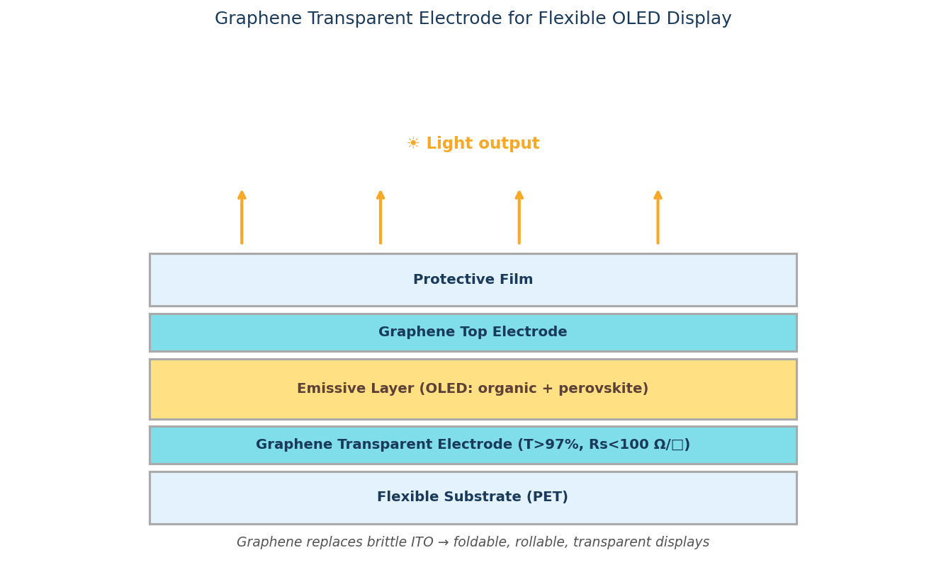
Replaces ITO — Graphene is a flexible, earth-abundant alternative to brittle indium tin oxide in transparent conductive electrodes
As our dependence upon renewable energy becomes more apparent, the need for efficient solar cells becomes more crucial, especially when they are one of the easiest and cheapest ways to generate clean energy. In general, solar cells are not that efficient. However, recent advances in graphene- based solar cells have seen the reflectance of solar rays reduced by 20%, which provides a potential efficiency increase up to 20%. There are currently many different variations of graphene-based solar cells being researched today.
This guide gives a comprehensive overview into the different types that are being investigated by academic and corporate researchers around the world.
Principles of Graphene Solar Cells
The basic principle of a graphene-based solar cell is essentially not that different from current inorganic/silicon solar cells being produced today, with the exception that some of the materials currently in use are replaced with graphene derivatives. As with any device or material, there are parameters that can be improved to increase operational efficiency. Graphene excels in tune-ability and adaptability.
For graphene-based solar cells, the two standout parameters that can potentially change the nature of the device are the number of graphene layers in the device (or in the individual components within a device) and the effects of doping a graphene-based material.
Effects of Graphene Layers in Solar Cells
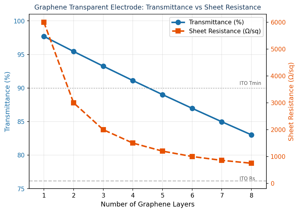
The relationship between optical transparency, sheet resistance, and the number of layers can be characterized by a proportional decrease in both the optical transparency and the sheet resistance, with an increasing number of graphene layers. A single layer of graphene shows an optical transparency of 97.7%. A 3-layered graphene stack exhibits around 90.8% optical transparency and the addition of each layer corresponds to a 2.3% decrease in optical transparency. A single sheet of graphene produces a sheet resistance of 2.1 kΩsq-1 and 350 Ωsq-1, while retaining 90% optical transparency.
The quenching effect of multiple graphene layers can be up to 11% greater than monolayer graphene, due to a higher hole accepting density.
Effects of Doped Graphene in Solar Cells
The doping of heteroatoms onto a sheet of graphene can significantly alter the chemical, physical, electronic and photonic properties of the sheet and is a common approach in many solar cells. There are two main types of doping- p-type and n-type. P-type doping utilizes trivalent atoms, such as boron, which extracts an electron off the graphene sheet and creates a hole, a process known as hole doping, where the hole is created in the valence band of the graphene sheet.
Whereas, n-type doping involves pentavalent atoms, such as phosphorous, and is an electron donating doping approach that facilitates a free electron from the pentavalent atom onto the graphene sheet. The free electron in this instance is facilitated in the conductance band of the graphene sheet. Doping a graphene sheet can occur through various methods, including through solid, liquid and gaseous phase chemical doping, ball milling, thermal annealing, in-situ doping during chemical vapor deposition (CVD) methods and plasma treatment, to name a few.
The effect of doping varies depending on both the type of graphene derivative used and the doping process. Regardless of which of these parameters (or both) are utilized in the doping process, the general result is improved efficiency of the solar cell.
Graphene-Silicon Solar Cells
OPV device with graphene anode: replaces brittle ITO for roll-to-roll printed, flexible organic solar cells.
Various allotropes of carbon have been implemented into solar cells to reduce the cost, allowing them to be more widely used. Other allotropes of carbon, have not been successful due to the inability to tune the electronic properties and the thickness of the layers. Graphene based films for solar cells can be produced with a predetermined thickness and complete coverage. It also allows the properties to be tuned, dependent upon the doping mixture used.
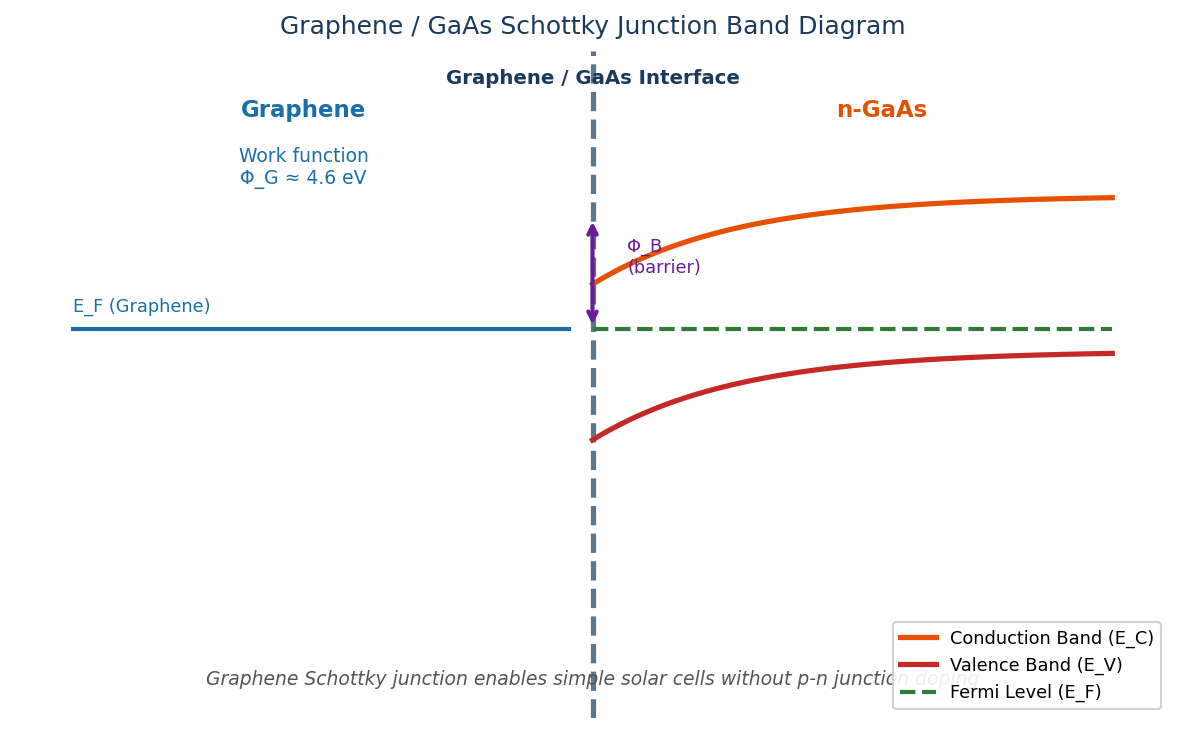
Graphene has now been implemented into various junctions in graphene-silicon solar cells, including p-type heterojunctions, n-type heterojunctions and Schottky junctions. Graphene-silicon solar cells are being researched however pure silicon cells performance is still superior. The tuneability of graphene is promising for hybrid solar cells. While it is not at the same level yet, advancements are being made and it is just a matter of time until their efficiency surpasses pure silicon cells. To date, n-type heterojunctions can generate a 0.55- 0.57 internal voltage to help facilitate electron-hole separation.
Schottky junctions have only showed a power conversion efficiency (PCE) of 1.5%, but the fill factor at present has only reached 56%, so theoretically, the efficiency can be vastly improved upon. Doping the graphene layers with gold particles has found to increase the efficiency by up to 40%.
Graphene-Polymer Solar Cells
Graphene/GaAs Schottky junction: simple device architecture without p-n junction doping, with graphene as transparent top electrode.
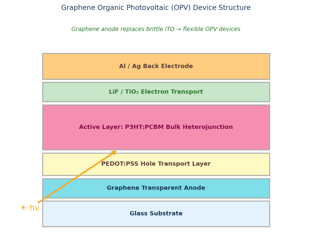
A highly researched area of graphene incorporation is in polymer-based solar cells. Polymeric materials offer many advantages over inorganic-based materials due to their tuneability, low-cost and simple fabrication processes. Graphene has shown great potential in transparent electrodes as a replacement for indium tin oxide (ITO) in polymer-based solar cells. The graphene in the electrode becomes an organic-inorganic hybrid material after it undergoes coating, layering, reduction and temperature annealing.
The hybrid material has a better energetic relationship, as the fermi-level of the graphene and the semi- conducting layer are closer together for an efficient charge injection. Graphene-polymer transparent electrodes also possess a high work function and conductivity, but it does have a limit of 65% light transmittance. In addition to reducing the graphene into hybrids, CVD-produced graphene can also be used as transparent electrodes. CVD-graphene is ozone treated, which produces carbonyl and hydroxyl functional groups on the surface of the graphene.
The oxygen based functional groups improves the open circuit voltage, but conductivity is reduced due to the sp2 hybridized covalent network being disrupted by sp3 bonds around the functionalized carbons. Non-covalent functionalized CVD-grown graphene shows a good conductivity and can have up to 0.55 V open circuit voltage, a fill factor of 55% and a PCE of 1.71%. The flexibility of graphene allows the solar cell to bend up to 78° more than pure ITO electrodes.
Electron transporter and acceptor based graphene-polymer solar cells rely on a high electron affinity to dissociate the electron-hole pairs into separate charges. Unlike other materials, graphene gives and effective separation when mixed with conjugated polymers. The large surface area of graphene allows for a continuous pathway and multiple donor/acceptor sites for efficient electron transfer. This type of solar cell has produced a PCE of 1.1%. A hole transport layer is required in many solar cells to stop current leaking and charge recombination.
Graphene can be mixed with polymeric material to produce a material with a band gap of up to 3.6 V which prohibits electron migration from the cathode to the anode. A 2nm graphene film is known to provide the best results as the thick film prevents the transmittance of electrons and increases electrical resistance. The highest PCE obtained has been 9 %, which is comparable, if not greater, than other materials used as hole transport layers.
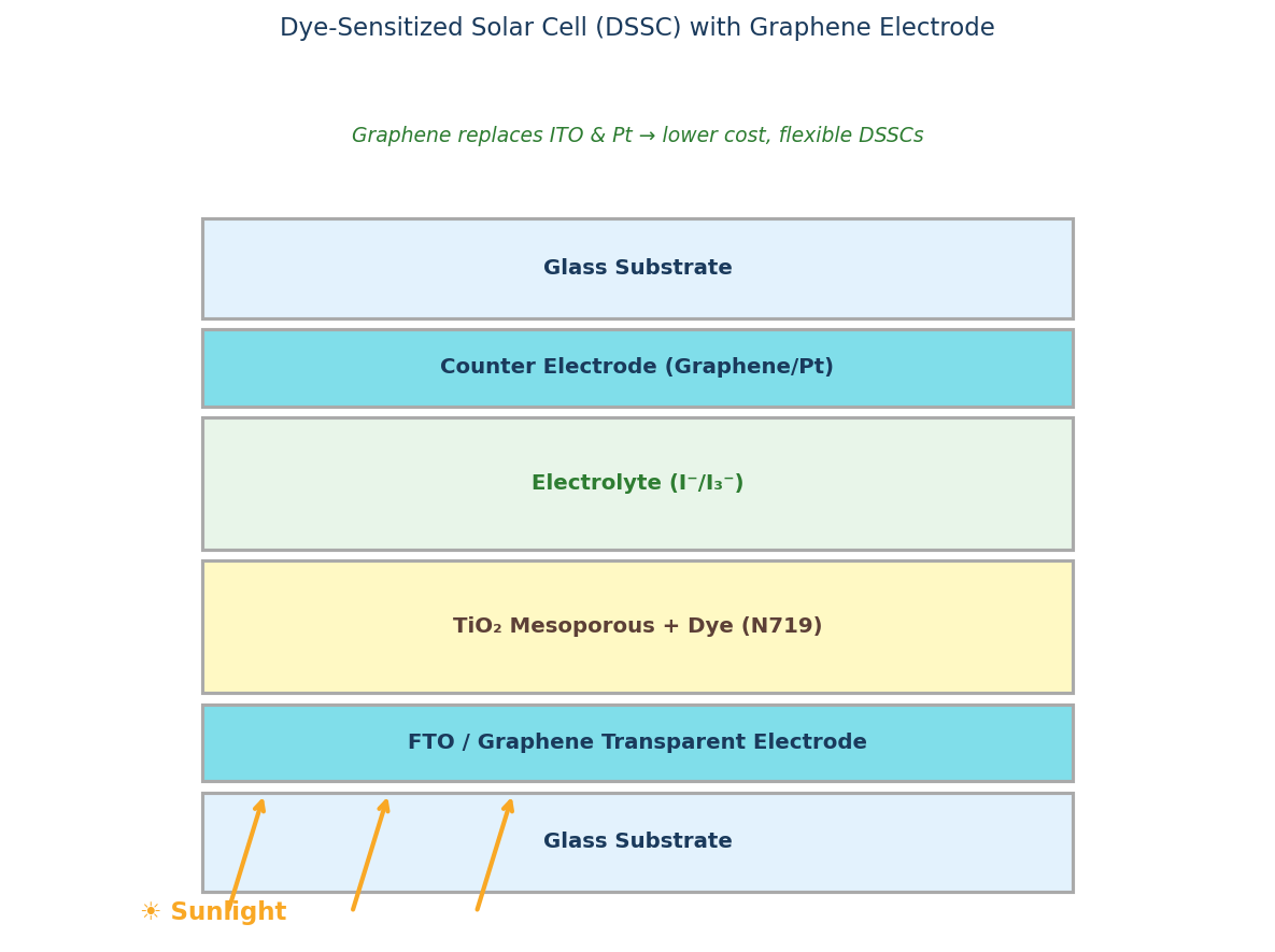
DSSC structure with graphene electrode: graphene replaces expensive ITO and Pt, enabling lower-cost, flexible dye-sensitized solar cells.
Dye Sensitized Solar Cells (DSSC’s)
Graphene transparent electrode performance: single-layer graphene offers ~97.7% transmittance, competing with ITO.
DSSC’s are different when compared to other types of solar cells. They contain a semi-conducting material (e.g. TiO2) with a photo-sensitive dye as the anode coupled with a pure metal cathode (e.g. Platinum) and an electrolyte solution. Graphene has many favourable properties that can increase the loading efficiency of the dye molecules, increase the interfacial area and improve the conductivity of the electrons to compete against the effects of charge recombination. Balancing the ratio of TiO2 and graphene is crucial to achieving an efficient system.
The valence electrons from graphene become excited into the TiO2 conduction band via the graphene-TiO2 interface, which efficiently separates the electrons and the holes. So, enough graphene is required (roughly 1%) to facilitate this separation, but the introduction of higher graphene concentrations into the matrix causes the transmittance to be reduced. The incorporation of graphene into DSSC’s improves the light scattering at the photoanode, efficiently disperses the dye molecules and provides an efficiency that is 39% greater than pure TiO2 electrodes.
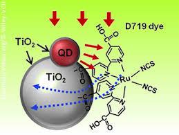
Graphene/Quantum Dot (QD) Solar Cells
Both graphene and carbon nanotubes have been hybridized with quantum dots to make functioning solar cells. Of the two carbon allotropes, graphene hybridized quantum dots have shown the most potential. Produced by electrophoretic and chemical bath deposition on ITO, a layered structure of both graphene layers and CdS quantum dots can be produced. The optimal layering structure consist of eight repeating graphene-CdS bilayers. This graphene-CdS configuration can produce and efficiency of up to 16%, which out performs carbon nanotubes-CdS by 7%, and 11% for other carbon allotropes.
This is attributed to graphene producing a better scaffold to incorporate the quantum dots, the layered structure provides a fast electron transfer from the QD to the graphene while suppressing the recombination of charges.
Graphene-Tandem Solar Cells
Tandem solar cells, otherwise known as multi-junction solar cells, are composed of two or more sub- cells that are stacked together in either a series or parallel configuration. It has been predicted that a single solar cell can theoretically produce up to 40% solar energy conversion efficiency, but tandem solar cells have the potential to reach up to 86% efficiency. The PCE of many solar cells has been enhanced to date by employing tandem arrangements.
The use of low band-polymer hybrid solar cells, commonly using ITO and other carbon derivatives, has been well studied, but graphene-based tandem solar cells are still a relatively new field. There has, however, been some promising developments using graphene oxide. Graphene tandem solar cells have not yet reached the heights of their non-graphene counterparts, but as a relatively new area they show great potential, especially as non-graphene tandem solar cells show relatively high PCEs.
One such development is that of a graphene oxide and polymer tandem solar cells that consist of 2 sub-cells. The cells consist of a bilayer of Cs-neutralized graphene oxide and pure graphene oxide connected by a charge recombinant layer of MoO3 and aluminium. Such cells have been found to produce a PCE between 2.92% and 3.91%, depending on the polymer blend used and the thickness of the different components within the cell.
The open circuit voltage of the cell can vary between 1.23 V and 1.69 V, but is dependent on the resistance of the interconnecting layer between the graphene oxide sheets, which is a function of the thickness of the layer. Another tandem cell that utilizes graphene also incorporates single-walled carbon nanotubes. Combinations of these materials have also been used as the hole transport and interconnecting layers for ITO-based sub-cells.
The thin film composed of these two carbon allotropes have been used in both regular and inverted solar cells, and the associated solar cells exhibit PCEs of up to 3.50% and 2.90%, respectively. The resulting solar cell possess a higher PCE than solar cells that contain the same sub-cells but lack the graphene connecting layers. Even though in this application they are not directly involved in the sub-cells, the presence of graphene in the device increases its overall efficiency.
Graphene-Perovskite Solar Cells (PSCs)
Perovskite solar cell with graphene electrodes — improves charge extraction and enables flexible substrates.
Perovskite solar cells (PSCs) have made great strides over the last few years due to their interesting bandgap and absorption properties that produce high PCEs. Perovskite solar cells have a standard structure, including the type of materials that are used, so the substitution of one material for another is a relatively simple process that leads to highly tuneable solar cell devices. Nanocomposites composed of anatase-TiO2 and graphene nanoflakes have shown promise with a PCE up to 15.6%.
The best results in these solar cells can be achieved when the nanocomposite is utilized as an n-type electron collection layer. The graphene is present as a monolayer and is only present as 0.6 wt% of the whole cell. Any amount above this drops the efficiency and is dependent upon a thin collecting layer. These perovskite solar cells can also be produced by low temperature sintering methods. These cells also possess short circuit and open circuit values of 12-21.9 mAcm-2 and 1.05 V, respectively.
When paired with an efficient light absorber, graphene oxide can be used as a hole conductor for inverted solar cells. The fabrication of this class of PSC is more complex in its synthesis, but provides a PCE between 9.26% and 11%, which is up to 7% greater than similar solar cells without the graphene oxide layer. Thinner layers of graphene oxide (2nm) can produce higher efficiencies. The average short and open circuit values in these solar cells are around 15.58 mAcm-2 and 0.99 V.
Similar solar cells to the previous example have been created, but by using reduced graphene oxide as a hole transport layer, with a light absorber material. These solar cells only reach a PCE maximum of 9.14%, but are much more stable and can retain 62% of their initial PCE after 140 hours of constant sun exposure. Thus out performing many other solar cells that can deteriorate significantly after 120 hours.
The higher stability is attributed to the increased resistance that reduced graphene oxide possess against oxygen and moisture compared to other graphene derivatives. One application of graphene oxide is to functionalize it with amphiphilic moieties to promote interface wettability on the surface of a perovskite solar cell. The modification of graphene oxide can reduce the contact angle of hole transporting layer solutions to 0°.
The carbon-carbon bonds in the graphene sheet absorb the hole transport layer molecules via p-p interactions and improve the both the interfacial interactions within the solar cell which leads to an improved performance. The functionalized graphene oxide can be doubled up as a buffer layer in PSCs and the dual-purpose graphene sheets can not only increase the short and open circuit potentials, but also increase the PCE of a PSC device by up to 45%. The graphene derrivative graphyne can be used in PSCs to achieve high results.
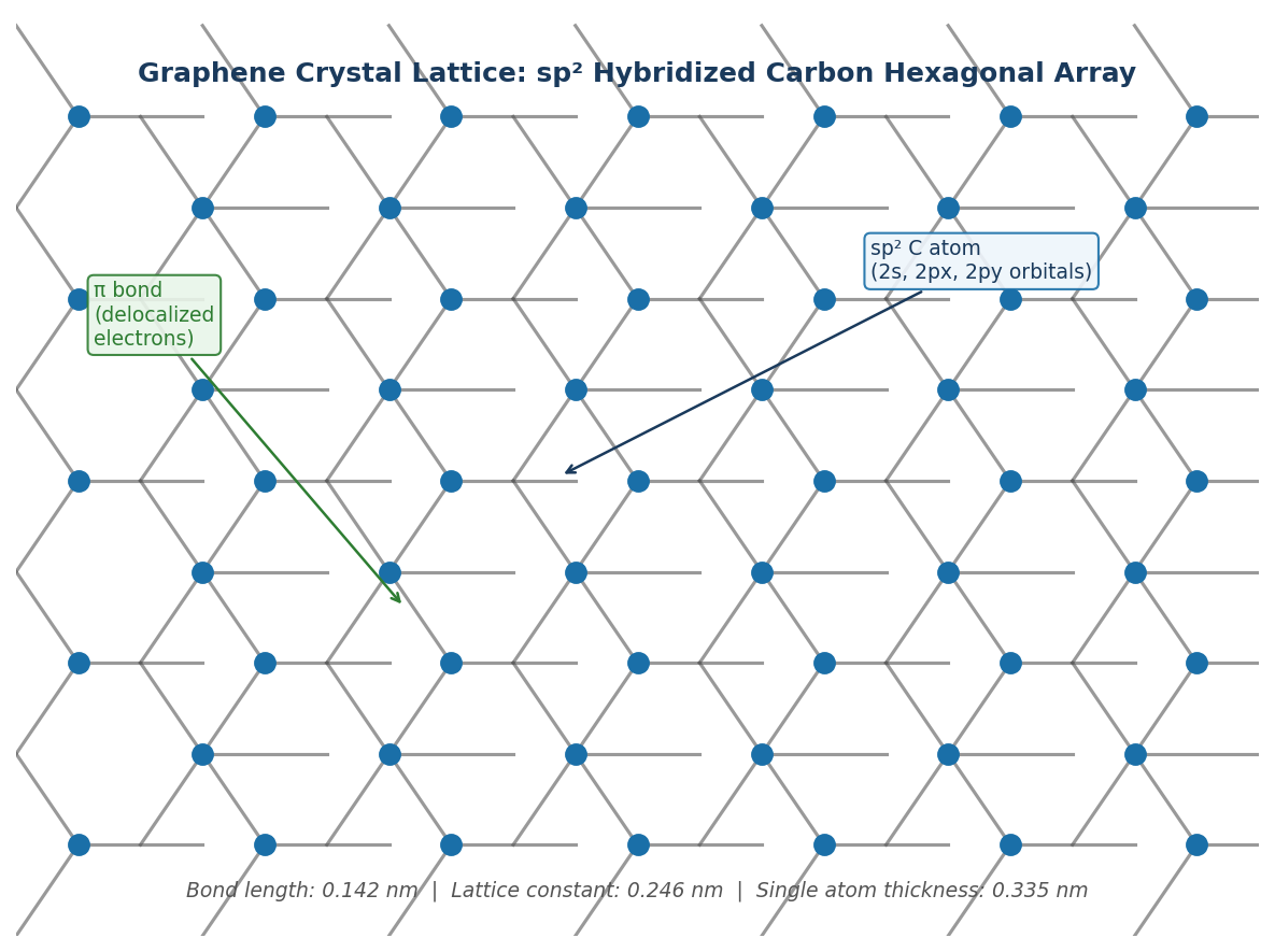
Graphyne is a 2D material similar to graphene, but unlike graphene’s structure of a regular hexagonal sp2 array, graphyne possess a mixture of sp and sp2 hybridised carbons and can be thought of as a lattice of phenyl rings connected by acetylene bonds, which arrange themselves as irregular hexagons. The incorporation of graphyne into hybrid electrodes, in an inverted solar cell, can achieve PCEs up to 14.8%- much higher than non-graphyne solar cells of a similar composition.
Graphene-Organic Solar Cells
While the main focus around solar cells generally tends to involve the different inorganic components, the organic components of the solar cell also play a major role. Organic and inorganic components in a solar cell have advantages and disadvantages, but the optimization of the organic components can produce a more efficient solar cell. Components that might traditionally be inorganic in nature are now being replaced with inorganic- organic hybrid materials that offer greater physical properties, solution-processability, cost-effective production, a large surface area, and are much lighter in nature.
One concern with many solar cells is the environmental stability, but organic molecules can provide stability against temperature, moisture and chemical degradation in solar cells, even when present as a hybrid material. The combination of organic and inorganic components generally produces higher stabilities and efficiencies than their pure predecessors. Aside from the two electrodes, traditional organic solar cells contain an active PEDOT:PSS layer and a donor-acceptor blend layer- commonly composed of P3HT or fullerenes (or both).
In recent years, the active PEDOT:PSS layer has been replaced by graphene derivatives and are generally used as hole-transport layers in organic solar cells. These components, while not specifically a class of their own, cover a wide range of solar cell applications nowadays, including in many heterojunction solar cells.
Graphene Bulk-Heterojunction Solar Cells
Graphene’s high electronic conductivity, transparency and flexibility make them useful in heterojunction solar cells, where they can be employed in many different ways including electrodes (both anodes and cathodes), acceptor layers, donor layers, buffer layers and active layers. The multijunction within the solar cell relies heavily on graphene’s specific tuneable parameters, including the thickness, thermal annealing temperature, the concentration of doping on the sheet and its photovoltaic performance. Graphene-heterojunction solar cells are by far the most widely studied and used graphene-based solar cell.
There are many variations of heterojunction solar cells and how graphene derivatives can be incorporated into them, including as transparent electrode, photoactive layers and Gallium Arsenide (GaAs) solar cells. As such, graphene heterojunction solar cells cannot be generalized as a single class of solar cells.
Graphene Transparent Electrodes
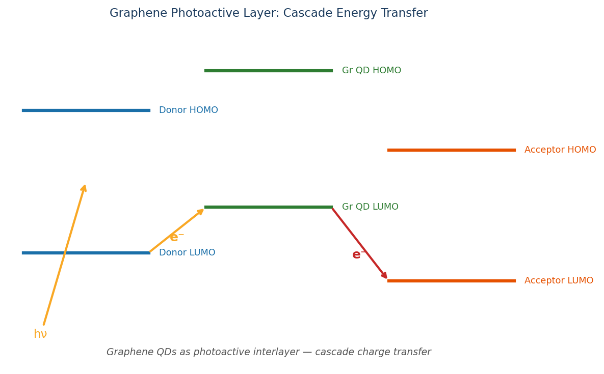
Graphene QDs as photoactive interlayer: cascade energy transfer from donor to acceptor improves photovoltaic efficiency.
Graphene can easily be incorporated into certain layers. Coupled with its excellent electrical, optical, mechanical, and thermal properties, this has allowed graphene to be studied as transparent electrodes in solar cells. We’ve explored a few of the different molecules employed in composite graphene transparent electrodes, but there are many others currently being researched. Prior to graphene being employed as a transparent electrode, ITO was the most commonly used material because of its high optical transparency. However, ITO is not cost effective, is brittle, and lacks mechanical flexibility.
Graphene exhibits a high optical transparency 90-100% and a low sheet resistance, even in multiple layered graphene stacks- both of which are great properties for transparent electrode applications. There have been many cases of graphene derivatives being employed as both the anode and the cathode in heterojunction solar cells. Some of the common molecules used in these graphene derivatives including polyethylene naphthalate (PEN), PEDOT, PSS, MoO3 and ZnO, to name a few.
PEDOT:PSS layers are the most common in graphene transparent electrdoes, with other materials being incorporated to improve and/or tune the properties. Using a graphene-based dual electrode system, flexible solar cells have been fabricated using different graphene derivations. PEN substrates containing various combinations of graphene, PEDOT:PSS, PTB and inorganic oxides generally show a PCE of 6.1-6.9% for the anode and 6.7- 7.1% for the cathode.
These solar cells have also been found to exhibit a short-circuit photocurrent density up to 14.8 mAcm-2, an open circuit voltage up to 0.71 V, with the potential to obtain a form factor of up to 57.6% after 100 tensile flexing cycles (or 20 flexing cycles). Solar cells from these composite dual graphene electrodes have found to show no loss of activity under mechanical tension binding tests, a high efficiency and excellent mechanical strength.
Another range of graphene bi-electrode solar cells incorporating PEDOT:PSS, copper and Buckminster fullerenes (C60) into the electrodes, where one electrode is doped with gold particles (in the form of gold (III) chloride). The doping of the graphene electrode changes the wetting in the PEDOT:PSS layer on the surface of the graphene sheet. The change in properties leads to an enhances PCE performance across the whole cell. Solar cells of this variety have been produced using 1-3 layers of graphene sheets.
The solar cells electrodes can have a sheet resistance between 300 and 500 Ωm-2, with a transmittance ranging between 91.2-97.1%. The PCE of such solar cells are found to be around 1.63%. The PSS can be replaced by polyethylene glycol (PEG) to produce a solar cell which is less corrosive in nature (PSS is a strong acid). However, compared to other cells, the PCE is much lower so it’s not generally used. An alternative to using PEDOT:PSS is MoO3.
This has been used by some researchers to produce a different kind of hole transport layer. In these cells, low pressure CVD-grown graphene is used as the graphene source. These cells consist of anode composed of graphene, MoO3, C60 and copper phthalocyanine (CuPc). This is a similar composition to many PEDOT:PSS electrodes and allows for a direct comparison in performance- one of the many reasons why the composition was chosen. Depending on the thickness of the hole transport layer, the PCE of these solar cells can range from 0.71-0.31%.
While the PEDOT:PSS reference cell exhibited a PCE of 0.85%, this cell class exhibit a much higher PCE than transition metal electrodes, where Mg/Al electrodes exhibit the highest at 0.56%. Another area of graphene transparent electrodes research explores zinc-graphene anodes. Some researchers have developed a hybrid photoanode, based around a P3HT, ZnO and ZnS core-shell nanorod array, suspended on a reduced graphene oxide film modified with ITO.
Each component has a specific function within the electrode, the P3HT acts the hole acceptor, the ZnS as the mediator and the ZnO is transporter and conductive collector. In these anodes, the PCE is enhanced by the presences of both a reduced graphene oxide film and ZnS/ZnO nanorods, showing a PCE greater than 1.01%. This is two and half times the PCE of the electrodes that don’t contain graphene, although still not as high as other solar cells.
There have also been many other attempts to improve the photovoltaic performance of both the transparent electrodes and the solar cells as a whole. Various multilayer electrodes based around graphene, gold, P3HT, PCBM, PEDOT:PSS, copper and PMMA in various compositions have been employed with significantly different results. The transparency of these electrodes varies from 82.3% to 90% with sheet resistances varying massively between 92 Ωm-2 and 374 Ωm-2. The PCE of such electrodes can vary between 1.17% and 13.3%.
Graphene Photoactive Layers
Both graphene and graphene oxide can also be employed in heterojunction solar cells as photoactive layers in the form of an active interfacial layer, electron-hole separation layer, hole-transport layer or as an electron-transport layer. As a general class of materials, graphene photoactive layers can exhibit a PCE from anywhere between 0.4 and 10.3% depending on the graphene derivative and the type of photoactive layer being produced. There are currently hundreds of graphene photoactive layers being employed as heterojunction solar cells.
Photoactive layers composed of a few layers of pure graphene films whether produced by CVD, flame pyrolysis, or other exhibit a PCE range between 1.01-2.88%. They can be employed as n-type heterojunctions by utilizing n-type type silicon alongside the graphene layers. Doping with nitric acid increases the PCE of these pure graphene heterojunctions up to 4.35%, where up to 4.18% of the PCE can be retained after 10 days.
Graphene can also be coated onto n-type silicon nanowire arrays, where the nanowires suppress and harvest light much better than their planar counterparts. However, they do show a lower PCE value than planar graphene-silicon heterojunctions, even after doping with thionyl chloride. Planar graphene-silicon solar cells can also be doped with thionyl chloride show a PCE lower than nitric acid doping, but greater than that of pure graphene-silicon heterojunctions with a PCE of 3.93%.
The highly volatile nature of thionyl chloride is responsible for the lower doping effects compared to nitric acid. The interface of the heterojunctions is the most important part and a single layer of CVD-grown graphene (97% transparency, 350 Ωm-2) on silicon can exhibit a PCE of 5.38-7.85%- much greater than multilayer graphene heterojunctions. This value can be increased even further to 8.94% by the incorporation of an antireflection layer of silicon dioxide. Aside from pure graphene, many graphene hybrid materials exist as photoactive layers.
One such example is that of lithium neutralized graphene oxide (GO-Li) as an interfacial layer between the photoactive layer and electron transport layer of solar cells. The incorporation of such layers can increase the PCE of a solar cell by up 6.29% compared to solar cells without the GO-Li layers. The thickness of these layers can tune the photovoltaic performance, with thicker layers producing a higher increase in the PCE. This layer also improves the stability of the solar cell under solar exposure, moisture and air.
Graphene quantum dots and crystalline silicon can be used as electron blocking layers to prevent charge carrier recombination at solar cell anodes. In these cells, surface passivation can occur due to differing terminal groups, namely, oxide, hydrogen and methyl moieties. Cells containing the methyl terminal group show the best PCE of up to 6.63%, compared to 2.24 and 2.92 for hydrogen and oxide terminal groups.
However, degradation can occur over time and the short circuit value can drop by more than 5 mAcm-2 and the PCE can drop by up 1.2%. Graphene oxide can be used with gold nanoparticles to produce anodic buffer layers. Capping agents are utilized in these hybrids, generally in the form of glycine or sodium citrate and can show a PCE ranging from 2.82-3.34%. However, the inclusion of P3HT and IBCA into the solar cell can increase the PCE up to 5.10%.
Graphene oxide nanoribbons (GORs) can be used a hole extraction layers in many solar cells. These layers have been developed to replace existing ITO-based materials and have so far managed to increase the PCE of a solar device from 2.20% to 4.19%. Aside from the PCE, the incorporation of GORs produce a lower sheet resistance and a higher shunt resistance compared to their ITO counterparts. Electron extraction materials in solar cell devices can be fabricated using Cs-neutralized graphene oxide.
Solar cells utilizing these materials have been found to exhibit PCEs up to 3.67%. However, more importantly, the photoactive layer has been found to operate independently to the electrode materials, in both normal and inverted devices. The charge neutralization ability of these materials can reverse the charge extraction properties in heterojunction solar cells. One of the most efficient graphene photoactive layers is produced from a hybrid material containing graphene oxide, PEDOT:PSS and n-type silicon nanowires.
The wt% of graphene oxide has a profound effect on the PCE of the device with the optimum concentration being 30%, which produces a PCE of up to 9.57%. In comparison, the substitution of silicon nanowires for planar silicon produces a massive drop in the PCE to 4.30%. These layers not only show a high optical transparency compared to non-graphene photoactive layers of a similar composition, but also exhibit a reduction in the exciton decay.
Graphene Schottky Junction GaAS Solar Cells
GaAs solar cells have been one of the most widely studied type of heterojunction, namely Schottky junction, solar cells. Despite the large amount of research, only a few have reached PCE levels comparable to that of other heterojunctions and PSCs. However, the ones which have achieved high PCEs are some of the most efficient graphene-based solar cells. GaAs has a superior band-gap to silicon, with a charge carrier mobility that is six times higher.
Theoretically, GaAs heterojunctions have the potential to produce efficient solar cells, but the devices currently being produced vary in quality. One of the cells that is less favorable than it’s high-flying counterparts is based around CVD-grown single and multilayer graphene on n-type GaAs substrates, which only shows a PCE of 1.95% and an open circuit voltage of 0.65 V. Another such example is that of pillar-array-patterned silicon substrate with graphene, which only shows a PCE up to 1.96%.
With nitric acid doping, the cell can achieve a PCE of up to 3.55%, but it’s still lower than many other solar cells. By comparison, a Schottky junction solar cell made from CdS nanowires and graphene has only achieved a PCE of 1.65%, showing that there is a wide range in terms of quality, not only with GaAs solar cells, but with Schottky junction solar cells in general.
Of the higher achievers, one example is that of a solar cell composed of an n-type silicon and TFSA- doped graphene Schottky junction. The synthesis approach is simple and a PCE of up to 8.6% can be achieved, which is 4.5 times higher than that of its un-doped counterpart and 6 times greater than other GaAs solar cells. The doping of TFSA on these devices not only increases their performance, but also enhances the stability of the device, compared to an un-doped version, to both oxygen and moisture.
One of the better-quality GaAs solar cells is that of a cell which is composed of a GaAs substrate and graphene, with a silicon nitride (SiNx) insulating layer and silver ‘fingers’. These solar cells have achieved much better efficiencies than many other solar cells, with PCEs varying between 10.4% and 15.5%. By optimizing the open circuit voltage, junction ideality factor, graphene resistance and the internal interfacial contact, there is a theoretical possibility to achieve a PCE of up to 25.8% with these solar cells.
Solar cells composed of graphene/semiconductor van der Waals Schottky diodes, with a tuneable gate and Fermi level, lead the way in terms of efficiency. The heterojunction utilizes a graphene- dielectric-graphene gate to achieve a PCE of up to 18.5%- much higher than other GaAs solar cells. The open circuit voltage, while not the best compared to other solar cell classes, is better than many other GaAs solar cells, with a value of 0.96 V.
Aside from producing a highly efficient solar cell, there are theoretical predictions that the PCE of these cells could be increased to 23.8%. The last two GaAs solar cells, show values close to commercially ready solar cells, and until recently, silicon-based solar cells had only reached a PCE of up to 22.5%. So, with a bit of optimization, and despite the discrepancies in quality over the whole class of solar cells, some GaAs could reach efficiencies comparable to commercial solar cells.
Recent developments in silicon-based solar cells has achieved a PCE of up to 26%, but this has only just been discovered and is currently confined to academic laboratories.
Frequently Asked Questions: Graphene Solar Applications
How does graphene improve solar cell efficiency?
Graphene improves solar cell efficiency through several mechanisms: it reduces reflectance of incoming solar rays by up to 20%, provides an ultra-transparent conductive electrode (97.7% optical transmittance for a single layer), enables faster charge carrier mobility than conventional materials, and can be doped to tune its electronic properties. These combined effects can yield a potential efficiency increase of up to 20% compared to traditional indium tin oxide (ITO) electrodes.
What types of solar cells benefit from graphene?
Graphene has demonstrated benefits across nearly every major solar cell architecture: graphene-silicon heterojunction cells, polymer solar cells, dye-sensitized solar cells (DSSCs), quantum dot solar cells, tandem solar cells, perovskite solar cells (PSCs), and organic solar cells. In each case, graphene typically serves as a transparent electrode, hole/electron transport layer, or active light-absorbing material depending on the cell design.
What is the advantage of graphene over indium tin oxide (ITO) in solar cells?
Graphene offers several advantages over ITO: it is mechanically flexible (enabling roll-to-roll fabrication of bendable solar panels), earth-abundant and lower-cost than indium (a scarce element), chemically stable, and can be deposited over large areas via CVD. ITO is brittle, expensive, and becoming a supply-constrained material as demand for transparent electrodes grows in displays and photovoltaics.
What is doped graphene and why is it used in solar cells?
Doped graphene has foreign atoms or molecules introduced into its carbon lattice to alter its electrical properties. P-type doping (with trivalent atoms like boron) creates electron holes in the valence band, while n-type doping (with pentavalent atoms like phosphorus) adds free electrons. In solar cells, doping enables graphene to act as a selective charge transport layer — extracting either holes or electrons from the absorber and blocking the opposite carrier — which reduces recombination and improves open-circuit voltage.
Are graphene solar cells commercially available?
As of 2024, graphene solar cells remain primarily in the research and pilot-production stage. Graphene-perovskite and graphene-silicon cells have achieved laboratory efficiencies competitive with commercial silicon panels, but large-scale manufacturing challenges — including uniform CVD graphene deposition and long-term stability — are still being solved. Graphene materials (including graphene oxide and reduced graphene oxide) used in solar cell research are commercially available from suppliers like Cheap Tubes Inc.
Graphene Solar Cells Design of Experiments
Graphene Transparent Electrode
To produce a graphene transparent electrode for heterojunction solar cells, first, produce or purchase CVD-grown graphene on copper foil. To prepare this electrode, a modified transfer method is needed. To transfer, deposit PMMA and cure, followed by etching of the copper foil with FeCl3 solution and rinse with deionized water three times. The next stage is to rinse the PMMA-graphene with deionized water and place on a glass substrate. Re-deposit one drop of PMMA onto the material, cure and remove the PMMA with acetone.
Dope the transferred graphene film with HNO3 vapor (69% concentration, 10 seconds). To fabricate the device itself, the preparation of a silicon wafer with PEDOT:PSS is required. Clean a silicon wafer with acetone, ethanol and deionized water for half an hour and treat through chlorination and alkylation. Incorporate PEDOT:PSS with DMSO (5 %wt) and Triton (1 %wt) and stir to ensure through mixing. The fabricate the cell itself, use physical vapor deposition (PVD) and deposit LiF (0.6 nm) and Al (200 nm) electrodes onto the back of the silicon wafer.
Spin-coat the PEDOT:PSS solution onto the silicon wafer and graphene-glass substrate (4000 rpm, 1 minute, 70-80 nm thickness). Anneal the organic films (125 °C, 30 minutes) in a glove box. Encapsulate the solar cell, using a clamp and AB glue to firmly stick the silicon wafer and the graphene-glass substrate together.
Graphene Ga/As Solar Cell
The promising Ga/As solar cell has the potential to be further optimized for commercial use. Firstly, purchase or grow CVD-graphene on copper foil. Next, remove the oxides on the Ga/As wafers by dipping them in HCl solution (10 %wt, 3 minutes) and attach gold contacts (60 nm thickness) onto the back surface of the wafer by thermal evaporation. Deposit a SiNx layer (80 nm) on top of the Ga/As surface by plasma enhanced CVD with a lithography-processed mask, to act as the insulating layer between Ga/As and graphene.
Open a window (active area) on the Ga/AS by dipping in HCl solution (10 %wt, 5 minutes) and rinse with deionized water. Treat the active area using NH3 plasma treatment (5 min with a 120 W 27.5 MHz RF generator). Transfer the graphene sheet onto the substrate using PMMA as a support. Remove the PMMA with acetone and paste silver onto the graphene, above the SiNx area, followed by annealing (120 °C, 5 minutes). Spin coat TFSA (bis(trifluoromethanesulfonyl)amide) to dope the graphene.
Add an antireflection layer- an electron beam evaporated Al2O3 film (68 nm thickness). To prepare the gate, transfer an extra layer of graphene onto the active area that is coated with Al2O3 by the same method as before. Remove the PMMA and paste the silver gate electrode onto the graphene gate, followed by annealing (120 °C, 5 minutes).
Graphene Solar Cells Future Advancements
Solar cells are a topic of intense research in academia and industry alike with new advancements being realized all the time. Most solar cells being produced utilize silicon and inorganic-based materials, which are at some point going to reach their limitation. The incorporation of organic molecules of graphene derivatives, low band-gap polymers, or both, are set to revolutionize the industry and lead to many commercially viable solar cell device architectures.
There has been tremendous progress so far into graphene-based solar cells and this is going to continue well into the future. The ability to optimize various parameters makes graphene-based solar cells highly tuneable and adaptable to future challenges in solar research.
Whether through improving existing solar cells, improving the properties of current non-graphene-based solar cells, or by creating a new range of graphene photovoltaics it is evident that graphene has a role in this exciting and rapidly advancing field. References: Huang X., Xiaoying Q., Boey F. and Zhang H., Graphene based composites, Chem Soc.
Rev., 2012, 41, 666-686 Singh E., Nalwa H., Graphene-based bulk-heterojunction solar cells: A Review, Journal of Nanoscience and Nanotechnology, 2015, 15, 6237-6278 Li P., Chen C., Zhang J., Li S., Sun B., Bao Q., Graphene-based transparent electrodes for hybrid solar cells, Frontiers in Materials, 2014, 1, 26 Guo X., Lu G., Chen J., Graphene-based materials for photoanodes in dye-Sensitized solar cells, Frontiers in Energy Research, 2015, 3, 50 Ye Y., Dai L., Graphene-based schottky junction solar cells, J. Mater.
Chem., 2012, 22, 24224 Feng T., Xie D., Lin Y., Zang Y., Ren T., Graphene based Schottky junction solar cells on patterned silicon-pillar-array substrate, App. Phys. Lett., 2011, 99, 233505 Jie W., Zheng F., Hao J., Graphene/gallium arsenide-based Schottky junction solar cells, App. Phys.
Lett., 2013, 103, 233111
Miao X.,
Tongay S.,
Petterson M.,
Berke K.,
Rinzler A.,
Appleton B.,
Hebard A., High Efficiency Graphene Solar Cells by Chemical Doping, Nano Lett., 2012, 12(6), 2745-2750
Li X.,
Zhang S.,
Wang P.,
Zhong H.,
Wu Z.,
Chen H.,
Liu C.,
Lin S., High performance solar cells based on graphene-GaAs heterostructures, Nano Energy, 2015, 16, 310
Li X.,
Chen W.,
Zhang S.,
Wu Z.,
Wang P.,
Xu Z.,
Chen H.,
Yin W.,
Zhong H., Lin S., 18.5% efficient graphene/GaAs van der Waals heterostructure solar cell, Nano Energy, 2015, 16, 310-319
Yoshikawa K.,
Kawasaki H.,
Yoshida W.,
Irie T.,
Konishi K.,
Nakano K.,
Uto T.,
Adachi D.,
Kanematsu M.,
Uzu H.,
Yamamoto K., Silicon heterojunction solar cell with interdigitated back contacts for a photoconversion efficiency over 26%, 2017, Nature Energy, 2, 17032
Mike Foley is the founder of Cheap Tubes Inc., a Vermont-based supplier of research-grade carbon nanomaterials since 2005.
He has a BS in Business Administration and a high-tech manufacturing background spanning wafer fabs, thin-film optics, and nanotechnology, with a pending patent application related to nanoparticle dispersion. Cheap Tubes supplies carbon nanotubes, graphene, graphene oxide, MXene, and specialty nanomaterials to researchers and engineers in 50+ countries.
This Guide to Graphene Synthesis, Properties, and Applications is intended to convey a general understanding of these topics for both Scientists & Non-Scientists alike.
Graphene: a single atom thick hexagonal lattice of sp² carbon — the thinnest, strongest, and most conductive material ever discovered.
Introduction To Graphene
Types & Forms of Graphene
To gain the benefits of graphene oxide, it is typically dispersed, added into a formulation, made into a film or other nano-enabled product and then reduced to restore the graphene structure.
Reduced Graphene Oxide (rGO)
There are many methods to reduce graphene oxide (GO) into reduced graphene oxide (rGO), but most fall into three main categories: chemical reduction, thermal reduction and electrochemical reduction.
The other methods include hydrazine vapor treatment, annealing, laser and microwave reduction. The reduction process is vital to producing rGO, as it determines how consistent the rGO structure is with the GO precursor.
Many commercial producers of Graphene Nanoplatelets are in fact providing a product similar to industrial scale rGO as their GNP product. However this method differs from the rGO most people refer to which is a higher quality research product used for nano enabled devices.
Chemical reduction is a scalable method but can often result in poor yields and utilizes highly toxic materials such as hydrazine. rGO produced by this method generally exhibits a low surface area and has a low conductivity compared to the GO precursor.
Thermal reduction produces rGO with a high surface area that is close to the surface area of pristine graphene. However, the intense heating process causes a high-pressure build-up of carbon dioxide which causes structural damage to the graphene layers.
The structural imperfections can then give rise to a reduction in the overall mass (and yield against the theoretical output), vacancies, voids and it can hinder the mechanical strength of the material.
Electrochemical reduction shows the best results in terms of production and quality. The rGO produced is consistent with that of pristine graphene.
During the electrochemical process, the substrates (generally ITO or glass) are coated with a layer of GO and a current is passed through the material (via electrodes at either end of the substrate). rGO produced by this method have shown to have a high carbon to oxygen ratio and have exhibited conductivity comparable to that of silver.
The process also benefits from no toxic waste. This process does however suffer from issues regarding the feasibility of the scalability of the method.
Graphene Nanoplatelets (GNPs)
GNRs can enhance the performance of lithium-ion batteries through edge chirality effects. GNRs have a band gap that is inversely proportion to their width, which is dependent upon their edge chirality.
Chirality occurs at the edges because the electron confinement potential deforms the wave-function and causes the electrons move in a single direction, with more weight in the ‘positive x’ direction. This leads to a current in the ‘positive y’ direction.
For electronic applications, the edges in GNRs have shown the best results when armchair and metallic edges are present due to their semi-conducting abilities. Armchair edges also reduce the band gap energy when there is a defined width.
The energy at the edges of GNRs is proportional to their density and armchair edges are more tightly packed at the graphene interface, so the energy is higher than that of zig-zag edges. Such edges can be produced on GNRs by electron beam irradiation and electron beam lithography.
A GNR with a high concentration and purity of armchair edges has been found to provide highly efficient p-n junctions in electronic devices.
Graphene Aerogels
Graphene aerogel: cross-linked graphene sheets form a 99% air porous network with SSA up to 1,100 m²/g — the lightest solid known, with excellent thermal insulation and conductivity.
Carbon aerogels are derived by sol-gel synthesis methods and are a unique class of high-surface-area materials. Their high mass-specific surface area, electrical conductivity, environmental compatibility, and chemical inertness make them very promising materials for many energy related applications.
Recent developments in controlling their morphology make them especially well suited to super capacitor applications.
Aerogels are a special class of open-cell foams that exhibit many unique and interesting properties, such as low mass density, continuous porosity and high surface areas. These properties are derived from the aerogel microstructure, which consists of three-dimensional networks of interconnected nanometer-sized particles.
Aerogels are typically prepared by sol–gel methods, a process that transforms molecular precursors into highly cross-linked inorganic or organic gels that can then be dried using techniques such as supercritical drying, freeze drying, ect to preserve the insubstantial solid network.
For organic and carbon aerogels, the transformation involves the polymerization of multi-functional organic species into three-dimensional polymer networks.
Graphene Masterbatches
Graphene masterbatch: GNP at 10–40% loading in a carrier resin, diluted to 1–5% for final composite processing — enables uniform dispersion in thermoplastics at industrial scale.
Graphene masterbatches are composite materials that contain a graphene-based compound (most commonly GO) and a polymer.
The graphene is used to enhance the properties of various common polymeric materials. Many polymers exhibit desirable properties such as low cost, low toxicity, bio-compatibility and chemical resistance, but they lack desirable mechanical properties.
By incorporating graphene nanoplatelets into polymer matrices, the polymers retain their original properties but benefit from enhanced rigidity and stiffness, while still being lightweight.
Using graphene as a filler compound rather than conventional inorganic materials can bring an enhanced electrical conductivity to the polymer, but it does have some issues.
In many graphene-based composites, graphene oxide acts as the dispersing support for other ions and molecules.
In polymer masterbatches, this can lead to problems as graphene doesn’t always disperse well in polymer phases (especially polyolefins) due to a lack of positive interactions at the grpahene polymer interface.
However, this can be overcome by the use of a surfactant, or by tailoring surface functionality of the graphene surface. The surfactant increases the surface interaction between the polymer and graphene.
If functionalized, the functional groups promote interaction between itself and the polymer molecules. If the functional groups aren’t compatible, you may observe what we call “islands of masterbatch” with easily observed islands of polymer in between well dispersed graphene-polymer masterbatches.
Properties Of Graphene
GO is highly dispersible in water and polar solvents due to oxygen functional groups; rGO favors NMP and DMF.
The properties of graphene are unique due to its all carbon structure and nanoscale geometry.
Electronic Properties
Flexible GFET on PET: graphene channel with ionic gel gate — carrier mobility >10,000 cm²/V·s on flexible substrates, enabling wearable electronics and foldable circuits.
Because graphene has a delocalized pi-electron system across the entirety of its surface, the movement of electrons is very fluid.
The graphene system also exhibits no band gap, due to overlapped pi-electrons, allowing for an easy movement of electrons without the need to input energy into the system.
The electronic mobility of graphene is very high and the electrons act like photons, with respect to their movement capabilities.
The electrons are also able to move sub-micrometer distances without scattering. From tests done to date the electron mobility has found to be in excess of 15,000 cm2V-1s-1, with the potential of producing up to 200,000 cm2V-1s-1.
The repeating structure of graphene makes it an ideal material to conduct heat in plane. Interplane conductivity is problematic and typically other nanomaterials such as CNTs are added to boost interplane conductivity.
The regular structure allows the movement of phonons through the material without impediment at any point along the surface. Graphene can exhibit two types of thermal conductivity- in-plane and inter-plane.
The in-plane conductivity of a single-layered sheet is 3000-5000 W m-1 K-1, but the cross-plane conductivity can be as low as 6 W m-1 K-1, due to the weak inter-plane van der Waals forces.
The specific heat capacity for graphene has never been directly measured, but the specific heat of the electronic gas in graphene has been estimated to be around 2.6 μ J g-1 K-1 at 5 K.
Mechanical Strength
Graphene composite applications: lightweight panels for aerospace, EMI shielding for electronics, structural body panels for automotive, and high-performance sporting equipment.
Graphene is one of the strongest materials ever discovered with a tensile strength of 1.3 x 10¹¹ Pa. In addition to having an unrivaled strength, it is also very lightweight (0.77 mgm-2).
The mechanical strength of graphene is unmatched and as such can significantly enhance strength in many composite materials.
Flexibility/Elasticity
The repeating sp2 hybridized backbone of graphene molecules allow for flexibility, as there is rotation around some of the bonds, whilst still providing enough rigidity and stability that the molecule can withstand changes in conformation and support other ions.
This is a very desirable property as there are not many molecules that can be flexible and supportive at the same time. In terms of its elasticity, graphene has found to have a spring constant between 1-5 Nm-1, with a Young’s modulus of 0.5 TPa.
Graphene nanoribbon band gap: narrower ribbons produce larger band gaps, enabling semiconducting behavior for transistor applications.
Applications of Graphene
There are many applications of graphene because it’s a revolutionary material. It has many applications replacing conventional materials as well as the ability to support applications previously not possible before the advent of 2D materials. The applications of Graphene are truly endless and many are yet to be conceived of yet.
Sensors
Graphene gas sensor: adsorbing molecules directly shift carrier density in the graphene channel — enabling single-molecule sensitivity at room temperature without heating.
The ideal sensor is able to detect minute changes in its surrounding environment. Due to the planar and consitent arrangement of atoms in a graphene sheet, every atom within the sheet is exposed to the surrounding environment.
This allows graphene to effectively detect changes in its surroundings at micrometer dimensions, providing a high degree of sensitivity.
Graphene is also able to detect individual events on a molecular level. Many of graphenes properties are beneficial in sensor applications; as such, graphene could be used in sensors in various fields including bio-sensors, diagnostics, field effect transistors, DNA sensors and gas sensors, to name a few.
Batteries
rGO battery anode: graphene combines Li intercalation with surface adsorption to reach 744 mAh/g — double graphite — while maintaining fast charge capability.
Graphene can be incorporated into both the anode or the cathode in various battery systems to increase the efficiency of the battery and improve the charge/discharge cycle rate.
The excellent electrical conductivity, surface area and dispersibility of graphene enhances the beneficial properties present in many traditional inorganic-based electrodes, whilst simultaneously relieving the electrodes of their limitations.
Due to its versatile nature, graphene has been incorporated into lithium-ion batteries, lithium-sulphur batteries, supercapacitors and fuel cells, of which there are multiple variations of each available on the market today.
Graphene OLED display: graphene transparent electrode (T>97%) replaces brittle ITO in flexible panels — enabling foldable phones, rollable TVs, and wearable displays.
Graphene is an ideal material for use in electron emission displays as it exhibits a high aspect ratio and the dangling bonds at either end of the sheet allow for efficient electron tunneling.
The linear disperisty that the graphene surface provides produces massless Dirac Fermions. When exposed to an electric field, the field emission liberated electrons avoid all back-scattering because their escape velocity is independent to their energy.
Graphene can turn-on an electric field at 0.1 V µm-2, with a field enhancement factor of up to 3700. This can increase up to 4500 in screen printed graphene films.
Structural Composites
Graphene is incorporated into various composites for applications where strength and weight are limiting factors, for example in the aerospace industry.
Graphene is being incorporated into many materials to make the existing material stronger and more lightweight. For the aviation industry, a composite material which is much lighter than steel but will still provide the necessary strength will save a lot of money on fuel consumption, which is why graphene has started to be incorporated into such materials.
Graphene-based structural composites have a huge potential to become a widely used alternative to many materials used today.
Catalyst Supports
Graphene-supported Pt catalyst: 3–5 nm Pt particles on graphene achieve 3–5× higher active surface area than carbon black, dramatically reducing precious metal requirements.
Even though the surface of graphene is planar and uniform, like any other material in existence it is subject to intrinsic defects.
Catalysts in the form of metal ions can sit in these cavities and be supported. In addition to providing mechanical support, the excellent charge carrier ability of graphene assists the charge transfer reactions involving the catalyst.
Graphene is also inert and does not interfere (in a negative way) with the interaction between the catalyst and the substrate materials. Graphene also provides an even dispersion of catalyst particles, so the catalyst-substate reaction is consistent across the whole support.
Polymer Masterbatches
Graphene can be incorporated into polymeric materials to form graphene-polymer composite materials.
As many polymeric materials suffer from strength-related problems, the incorporation of graphene can help to increase the tensile strength of the polymers, increasing the shelf life of the polymeric material in commercial applications.
Incorporating graphene into polymers can also give polymers electrical conductivity properties.
Functional Inks
Graphene can be used in functional inks for electronic, heat resistant and anti-corrosion purposes. By incorporating graphene into ink formulations, the conductivity properties associated with graphene influence the ink, causing it to become conductive.
The inks can then be used to coat electronics. Compared to other conducting inks, graphene is non-toxic, environmentally friendly, cheaper, quick-drying and recyclable. Graphene also has a high thermal stability, making it an ideal for heat resistant ink coating in electronic applications that produce large amounts of heat.
It is also an ink of choice when processing temperatures need to be high, as the graphene won’t break down during the manufacturing process. Graphene also exhibits excellent chemical stability and is inert.
For applications where environmental factors are an issue, graphene inks can provide a stable barrier to protect materials from chemicals and corrosion.
We hope you enjoyed this guide and found it informative. Graphene’s next killer app could be Your’s.
References:
Huang X., Xiaoying Q., Boey F. and Zhang H., Graphene based composites, Chem Soc. Rev., 2012, 41, 666-686
Zhou G., Yin L., Wang D. and Cheng H., A fibrous hybrid of graphene and sulfur nanocrystals for high performance lithium-sulfur batteries, ACS Nano, 2013, 7(6)
Cheng Q., Tang J., Zhang H., Graphene and carbon nanotube composite electrodes for supercapacitors with ultra-high energy density, Phys. Chem. Chem. Phys., 2011, 13, 17615-17624
Peng Z., Xiang C., Yan Z., Natelson D., Graphene Nanoribbon and Nanostructured SnO2 Composite Anodes for Lithium Ion Batteries, ACS Nano, 2013, 7(7)
Haegyeom K., Dong-Hwa S., Sung Wook None K., Kisuk K., Highly reversible Co3O4/graphene hybrid anode for lithium rechargeable batteries, Carbon, 2011, 49(1), 326-332
Bak S., Kim D., Lee H., Graphene quantum dots and their possible energy applications: A review, Current Applied Phyics, 2016, 11, 1192-1201
Liu Y., Dobrinksy A., Yakobson B. I., Graphene edge from armchair to zigzag: The origins of nanotube chirality, Phys. Rev. Lett., 2010, 105, 235502
Begliarbekov M., Sasaki K., Sul O., Yang E., Strauf S., Nano Lett., 2011, 11(11), 4874-4878
Pop E., Varshney V., Roy A., Thermal properties of graphene: Fundamentals and applications, MRS bulletin, 2012, 37, 1273-1281
Lei W., Li C., Cole M., Qu K., Ding S., Zhang Y., Warner J., Zhang X., Wang B., Milne W., A graphene -based large area surface-conduction electron emission display, Carbon, 2013, 56, 255-263
We supply CVD graphene films, graphene oxide, reduced graphene oxide, and graphene nanoplatelets — every material covered in this guide. Consistent quality, CoA with every order, and technical support from a team with 20 years in nanomaterials.
Mike Foley is the founder of Cheap Tubes Inc., a Vermont-based supplier of research-grade carbon nanomaterials since 2005.
He has a BS in Business Administration and a high-tech manufacturing background spanning wafer fabs, thin-film optics, and nanotechnology, with a pending patent application related to nanoparticle dispersion. Cheap Tubes supplies carbon nanotubes, graphene, graphene oxide, MXene, and specialty nanomaterials to researchers and engineers in 50+ countries.
N2 Functionalized Multi Walled Carbon Nanotubes 20nm
Our N2 Functionalized Multi Walled Carbon Nanotubes 20nm is produced by CCVD and is further purified and functionalized using a Dielectric Barrier Discharge process which provides greater control over the specific type & amount of surface functionality. DBD produces an exfoliated product that is much easier to disperse in the host matrix. Carbon Nanotubes have proven to offer a unique properties of stiffness and strength largely due to their high aspect ratio and all carbon structure. The thermal and electrical conductivity found in carbon nanotubes is very high compared to other conductive or fibrous additive materials. Select a functionalized product when trying disperse carbon nanotubes into certain host matrices to assist in dispersion. Carbon nanotubes are the clear choice when compared to other fiber additive materials. The introduction of nitrogen containing functional groups onto the CNTs surface is known to promote faradaic pseudocapacitive reactions. Among these functional groups pyridinic and pyrrolic enhance the capacitive behavior, while quaternary nitrogen and pyridinic-N-oxide improves electron transfer.
N2 Functionalized Multi Walled Carbon Nanotubes 20nm Specifications
F Functionalized Multi Walled Carbon Nanotubes 20nm
F Functionalized Multi Walled Carbon Nanotubes 20nm is produced by CCVD and is further purified or functionalized using a Dielectric Barrier Discharge process which provides greater control over the desired type & amount of Fluorine (a halogen) functionality which produces an exfoliated product that is much easier to disperse in the host matrix. Carbon Nanotubes have proven to offer a unique properties of stiffness and strength largely due to their high aspect ratio and all carbon structure. The thermal and electrical conductivity found in carbon nanotubes is very high compared to other conductive or fibrous additive materials. Select a functionalized product when trying disperse carbon nanotubes into certain host matrices to assist in dispersion. Carbon nanotubes with fluorine surface functionality stands out when compared to other fiber additive materials. Fluorinated carbon nanotubes are known to be a good starting point for further sidewall derivatization of the sidewall with other molecules. These secondary reactions involving substituting the Fluorine atom from the sidewall have been utilized to produce C-N bond formation, free radical addition, and cycloaddition.
F Functionalized Multi Walled Carbon Nanotubes 20nm Specifications
O Functionalized Multi Walled Carbon Nanotubes 20nm
Our O Functionalized Multi Walled Carbon Nanotubes 20nm is produced by CCVD and is further purified or functionalized using a Dielectric Barrier Discharge process which provides greater control over the desired type & amount of functionality which produces an exfoliated product that is much easier to disperse in the host matrix. The introduction of oxygen groups promotes dispersion in aqueous solutions but does not mean they are water soluble. Surfactants may be needed to stabilize dispersions in DI Water or other aqueous solvent mixtures.
O Functionalized Multi Walled Carbon Nanotubes 20nm Specifications
COOH Functionalized Multi Walled Carbon Nanotubes 20nm
Our COOH Functionalized Multi Walled Carbon Nanotubes 20nm is produced by CCVD and is further purified and functionalized using a Dielectric Barrier Discharge process which provides greater control over the specific type & amount of surface functionality. DBD produces an exfoliated product that is much easier to disperse in the host matrix. Carbon Nanotubes have proven to offer a unique properties of stiffness and strength largely due to their high aspect ratio and all carbon structure. The thermal and electrical conductivity found in carbon nanotubes is very high compared to other conductive or fibrous additive materials. Select a functionalized product when trying disperse carbon nanotubes into certain host matrices to assist in dispersion. Carbon nanotubes are the clear choice when compared to other fiber additive materials. The introduction of COOH groups is useful when working with paints, polymers, epoxies and inks.
COOH Functionalized Multi Walled Carbon Nanotubes 20nm Specifications
MWNTs Outer Diameter: <20nm
MWNTs Inside Diameter: 4nm
MWNTs Ash:0 wt%
MWNTs Purity: >99 wt%
MWNTs Length: 1-15um
Product MWCNTs
Process Gas: Oxygen Blend
Primary Functionality: COOH
Other Functionalities: COH, C=O, Other Oxygen Groups
NH2 Functionalized Multi Walled Carbon Nanotubes 20nm
NH2 Functionalized Multi Walled Carbon Nanotubes 20nm is produced by CCVD and is further purified or functionalized using a Dielectric Barrier Discharge process which provides greater control over the desired type & amount of Amine functionality and produces an exfoliated product that is much easier to disperse in the host matrix. Carbon Nanotubes have proven to offer a unique properties of stiffness and strength largely due to their high aspect ratio and all carbon structure. The thermal and electrical conductivity found in carbon nanotubes is very high compared to other conductive or fibrous additive materials. Select a functionalized product when trying disperse carbon nanotubes into certain host matrices to assist in dispersion. Carbon nanotubes with amine surface functionality stands out when compared to other fiber additive materials. The amino termination allows further chemistry of the functionalized carbon nanotubes and makes possible covalent bonding to polymers and biological systems such as DNA and carbohydrates.
NH2 Functionalized Multi Walled Carbon Nanotubes 20nm Specifications
This product is produced by CCVD and is further purified or functionalized using a Dielectric Barrier Discharge process which provides greater control over the desired type & amount of functionality which produces an exfoliated product that is much easier to disperse in the host matrix.
NH2 Functionalized Single Wall-Double Walled Carbon Nanotubes
Our NH2 Functionalized Single Wall-Double Walled Carbon Nanotubes is produced by CCVD and is further purified or functionalized using a Dielectric Barrier Discharge process which provides greater control over the desired type & amount of functionality which produces an exfoliated product that is much easier to disperse in the host matrix. The amino termination allows further chemistry of the functionalized carbon nanotubes and makes possible covalent bonding to polymers and biological systems such as DNA and carbohydrates. Carbon Nanotubes have proven to offer a unique properties of stiffness and strength largely due to their high aspect ratio and all carbon structure. The thermal and electrical conductivity found in carbon nanotubes is very high compared to other conductive or fibrous additive materials. Select a functionalized product when trying disperse carbon nanotubes into certain host matrices to assist in dispersion.
NH2 Functionalized Single Wall-Double Walled Carbon Nanotubes Specifications
Our Multi Walled Carbon Nanotubes 20nm are made by CCVD and purified and functionalized using concentrated acid chemistry. Carbon Nanotubes (CNTs) have proven to offer a unique properties of stiffness and strength largely due to their high aspect ratio and all carbon structure. The thermal and electrical conductivity found in CNTs is much higher than that of other conductive or fibrous additive materials. Surfactants are used to stabilize dispersions in DI Water or other aqueous solvent mixtures. The most common surfactants used are PVP, SDS, or SDBS. The carbon atoms in CNTs are arranged in a planar honeycomb lattice structure in which each atom is connected via a strong chemical bond to the three neighboring atoms. These strong bonds are the reason that the basal plane elastic modulus of graphite is one of the largest of any known material. Having such strong bonds at the atomic level as well as a high aspect ratio, Carbon Nanotubes are expected to be the ultimate high-strength fibers.
Multi Walled Carbon Nanotubes 20nm Specifications
This product is produced by CCVD and is further purified or functionalized using a Dielectric Barrier Discharge process which provides greater control over the desired type & amount of functionality which produces an exfoliated product that is much easier to disperse in the host matrix.
COOH Functionalized Single Walled-Double Walled Carbon Nanotubes 99
Our COOH Functionalized Single Walled-Double Walled Carbon Nanotubes 99 are made by CCVD and purified and functionalized using concentrated acid chemistry. Carbon Nanotubes (CNTs) have proven to offer a unique properties of stiffness and strength largely due to their high aspect ratio and all carbon structure. The thermal and electrical conductivity found in CNTs is much higher than that of other conductive or fibrous additive materials. Surfactants are used to stabilize dispersions in DI Water or other aqueous solvent mixtures. The most common surfactants used are PVP, SDS, or SDBS. The carbon atoms in CNTs are arranged in a planar honeycomb lattice structure in which each atom is connected via a strong chemical bond to the three neighboring atoms. These strong bonds are the reason that the basal plane elastic modulus of graphite is one of the largest of any known material. Having such strong bonds at the atomic level as well as a high aspect ratio, Carbon Nanotubes are expected to be the ultimate high-strength fibers. This product is produced by CCVD and is further purified or functionalized using a Dielectric Barrier Discharge process which provides greater control over the desired type & amount of functionality which produces an exfoliated product that is much easier to disperse in the host matrix.
COOH Functionalized Single Walled-Double Walled Carbon Nanotubes Specifications 99
Outer Diameter: 1-4nm
Inside Diameter: 0.8-1.6nm
Length: 3-30um
Ash: <1.5 wt%
Purity: >99 wt%
Additional MWNT content: >5wt%
Amorphous Carbon Content: <3wt%
Length: 5-30um
Specific Surface Area: 407 m2/g
Electrical Conductivity: >100 S/cm
COOH Functionalized SWNTs contain 2.7% COOH groups
Bulk density: 0.14 g/cm3
True density: ~2.1 g/cm3
Cited in research: Used by Tai & Lubineau (KAUST) in a heating-rate-triggered 3D conducting SWCNT/PEDOT:PSS transparent conductive film for noncontact moisture sensing. Read the Ultra-Long SWCNT TCF Launch Spotlight — Tai & Lubineau, Scientific Reports 6, 19632 (2016).
O Functionalized Single Walled-Double Walled Carbon Nanotubes 99
Our O Functionalized Single Walled-Double Walled Carbon Nanotubes 99 are made by CCVD and purified and functionalized using concentrated acid chemistry. Carbon Nanotubes (CNTs) have proven to offer a unique properties of stiffness and strength largely due to their high aspect ratio and all carbon structure. The thermal and electrical conductivity found in CNTs is much higher than that of other conductive or fibrous additive materials. Surfactants are used to stabilize dispersions in DI Water or other aqueous solvent mixtures. The most common surfactants used are PVP, SDS, or SDBS. The carbon atoms in CNTs are arranged in a planar honeycomb lattice structure in which each atom is connected via a strong chemical bond to the three neighboring atoms. These strong bonds are the reason that the basal plane elastic modulus of graphite is one of the largest of any known material. Having such strong bonds at the atomic level as well as a high aspect ratio, Carbon Nanotubes are expected to be the ultimate high-strength fibers. This product is produced by CCVD and is further purified or functionalized using a Dielectric Barrier Discharge process which provides greater control over the desired type & amount of functionality which produces an exfoliated product that is much easier to disperse in the host matrix.
O Functionalized Single Walled-Double Walled Carbon Nanotubes Specifications 99
This product is now supplied at a substantially improved specification. The new material is pure single-walled (1-2 nm outer diameter), 99.5% ± 0.5% purity, with ≥100 μm tube length — an order of magnitude longer than the prior 5-30 μm supply. Specific surface area 800-1,400 m²/g (near the theoretical SWCNT maximum), with low metal-catalyst residue and a six-year shelf life. See the launch Spotlight for the full context, including head-to-head comparison against ultra-long CNT specialty suppliers and OcSiAl TUBALL.
TEM micrographs, Raman spectra (RBM mode confirmation), and batch-specific Certificate of Analysis are added to product documentation as characterization is completed. Contact us for the latest QC package.
Stretchable conductors, percolation networks, conductive composites at low loading — the high aspect ratio (50,000:1 to 100,000:1) lowers percolation threshold.
Sensors, electrochemistry, fuel cell catalysis support — high SSA with low metal contamination for clean electrochemical baselines.
About the New Material
This is a next-generation single-walled carbon nanotube material delivering a substantial step-change in spec relative to the prior product line: pure single-walled chemistry, an order-of-magnitude longer tube length, near-theoretical specific surface area, and low residual metal content. The product is delivered as a dry black powder with uniform color and no hard lumps, packaged in a nano-suitable airtight container.
The combination of ≥100 μm tube length with 1-2 nm outer diameter gives an aspect ratio of 50,000:1 to 100,000:1 — among the highest in the commercial SWCNT supply chain. High aspect ratio is the single property that most directly improves the performance trade-off between conductivity and loading: longer tubes form percolating networks at lower volume fraction, which means lower mass for the same conductivity, less optical absorption in transparent applications, and better mechanical reinforcement at lower weight penalty.
Specific surface area of 800-1,400 m²/g approaches the theoretical maximum for single-walled carbon nanotubes (~1,315 m²/g), which is consistent with the purity claim — surface area drops sharply when amorphous carbon or multi-wall content is present. Residual metal impurity is low: Fe ≤ 5,000 ppm, Ni ≤ 600 ppm, Co ≤ 1,000 ppm — meaningfully lower than typical industrial-scale SWCNT supply where Fe routinely runs ~3 wt%.
Dispersion and Handling
Single-walled carbon nanotubes form tight bundles held together by van der Waals attraction. Dispersing them into a workable suspension requires breaking those bundles while protecting against re-bundling. Standard methods:
Aqueous dispersion (research scale): tip-sonicate at 10-30 W/mL for 30-60 minutes in DI water with a surfactant such as SDS, SDBS, or sodium cholate (0.5-2 wt%); follow with mild centrifugation (10,000 g, 10-20 min) to remove residual bundles. PVP and CMC also work for matrix-compatible formulations.
Solvent dispersion: NMP, DMF, and DMSO disperse pristine SWCNT without surfactant at low concentration (typically <0.5 mg/mL). For higher loading, use a surfactant-assisted route in water and exchange solvent post-dispersion.
Polymer composites: three-roll milling or planetary mixing for high-viscosity systems; high-shear mixing (5,000-20,000 RPM) for low-viscosity resins. For aqueous-processable polymer hosts like PEDOT:PSS, use the COOH or OH variants (in stock soon) for surfactant-free dispersion.
For functionalized chemistry needs: the COOH, NH₂, and OH variants of this material are being qualified and will be re-listed as available stock arrives. Contact us for samples and timeline.
Storage and Shelf Life
Sealed dry storage at room temperature. Stability testing supports a 6-year shelf life in the airtight container as shipped. Avoid prolonged air exposure once opened — pristine SWCNTs can pick up moisture and trace surface oxidation over time. Re-seal between uses; aliquot for high-frequency use to minimize headspace exchange.
Documentation
Every shipment includes:
Safety Data Sheet (SDS) — OSHA HCS / GHS format.
Technical Data Sheet (TDS) — representative purity, length, diameter, BET surface area, metal impurity.
Certificate of Analysis (COA) — batch-specific, available on request.
Sample-batch SEM and TEM micrographs — added to product documentation as the characterization package is finalized. Contact us for the latest QC package.
Samples are available on request for buyers evaluating the material against a specific application requirement.
Cited in research: Used by the Reichmanis group (Lehigh + Brookhaven National Lab + Stony Brook) as the SWCNT component of a stress-relieving PPBT/SWCNT coating for stable silicon microparticle anodes — 1,894 mAh/g reversible capacity at 300 cycles. Read the Si-Anode Spotlight — Gueon et al., ACS Applied Energy Materials 7(17), 7220-7231 (2024).
Our N2 Functionalized Graphene Nanoplatelets consist of small stacks of graphene that can replace carbon fiber, carbon nanotubes, nano-clays, or other compounds in many composite applications. When added in trace amounts to plastics or resins, our graphene nanoplatelets make these materials electrically or thermally conductive and less permeable to gasses, while simultaneously improving mechanical properties like strength, stiffness, or surface toughness. They are useful as nanoscale additives for advanced composites, as a component in advanced batteries and ultra/super capacitors, as the conductive component in specialty coatings or adhesives, and as a component of e-inks or printable electronic circuits. Other applications include exceptionally strong and impermeable packaging, better lubricants, and a recent publication even demonstrates that our conductive graphene nano-platelets, surface-treated with sensitized molecules, can be used to produce highly sensitive bio-sensors. The introduction of nitrogen containing functional groups onto the N2 Functionalized Graphene Nanoplatelets surface is known to promote faradaic pseudocapacitive reactions. Among these functional groups pyridinic and pyrrolic enhance the capacitive behavior, while quaternary nitrogen and pyridinic-N-oxide improves electron transfer.
Our GNPs consist of several sheets of graphene with an overall thickness of approximately 3-10 nanometers depending on the specific product. Grade 4 GNPs are friable to <4nm thick when exposed to high shear or sonication.
This product is produced by exfoliating natural graphite and is further purified or functionalized using a Dielectric Barrier Discharge process which provides greater control over the desired type & amount of functionality which produces an exfoliated product that is much easier to disperse in the host matrix.
Our SI Decorated Graphene Nanoplatelets consist of small stacks of graphene that can replace carbon fiber, carbon nanotubes, nano-clays, or other compounds in many composite applications. When added in trace amounts to plastics or resins, our graphene nanoplatelets make these materials electrically or thermally conductive and less permeable to gasses, while simultaneously improving mechanical properties like strength, stiffness, or surface toughness. They are useful as nanoscale additives for advanced composites, as a component in advanced batteries and ultra/super capacitors, as the conductive component in specialty coatings or adhesives, and as a component of e-inks or printable electronic circuits. Other applications include exceptionally strong and impermeable packaging, better lubricants, and a recent publication even demonstrates that our conductive graphene nano-platelets, surface-treated with sensitized molecules, can be used to produce highly sensitive bio-sensors.
Our Silicon doped graphene nanoplatelets consist of several sheets of graphene with an overall thickness of approximately 3-10 nanometers depending on the specific product. Grade 4 GNPs are <4nm thick.
This product is produced by exfoliating natural graphite and is further purified or functionalized using a Dielectric Barrier Discharge process which provides greater control over the desired type & amount of functionality which produces an exfoliated product that is much easier to disperse in the host matrix.
SI Decorated Grade 4 Graphene Nanoplatelets – GNPs Specifications
Our F Functionalized Graphene Nanoplatelets consist of small stacks of graphene that can replace carbon fiber, carbon nanotubes, nano-clays, or other compounds in many composite applications. When added in trace amounts to plastics or resins, our graphene nanoplatelets make these materials electrically or thermally conductive and less permeable to gasses, while simultaneously improving mechanical properties like strength, stiffness, or surface toughness. They are useful as nanoscale additives for advanced composites, as a component in advanced batteries and ultra/super capacitors, as the conductive component in specialty coatings or adhesives, and as a component of e-inks or printable electronic circuits. Other applications include exceptionally strong and impermeable packaging, better lubricants, and a recent publication even demonstrates that our conductive graphene nano-platelets, surface-treated with sensitized molecules, can be used to produce highly sensitive bio-sensors. The introduction of nitrogen containing functional groups onto the N2 Functionalized Graphene Nanoplatelets surface is known to promote faradaic pseudocapacitive reactions. Among these functional groups pyridinic and pyrrolic enhance the capacitive behavior, while quaternary nitrogen and pyridinic-N-oxide improves electron transfer.
Our GNPs consist of several sheets of graphene with an overall thickness of approximately 3-10 nanometers depending on the specific product. Grade 4 GNPs are friable to <4nm thick when exposed to high shear or sonication.
This product is produced by exfoliating natural graphite and is further purified or functionalized using a Dielectric Barrier Discharge process which provides greater control over the desired type & amount of functionality which produces an exfoliated product that is much easier to disperse in the host matrix.
This Product Has Been Discontinued 06-15-22. Do not order.
F Functionalized Grade 4 Graphene Nanoplatelets Specifications
Our NH2 Functionalized Graphene Nanoplatelets consist of small stacks of graphene that can replace carbon fiber, carbon nanotubes, nano-clays, or other compounds in many composite applications. When added in trace amounts to plastics or resins, our amine graphene nanoplatelets make these materials electrically or thermally conductive and less permeable to gasses, while simultaneously improving mechanical properties like strength, stiffness, or surface toughness. They are useful as nanoscale additives for advanced composites, as a component in advanced batteries and ultra/super capacitors, as the conductive component in specialty coatings or adhesives, and as a component of e-inks or printable electronic circuits. Other applications include exceptionally strong and impermeable packaging, better lubricants, and a recent publication even demonstrates that our conductive graphene nano-platelets, surface-treated with sensitized molecules, can be used to produce highly sensitive bio-sensors.
Our GNPs consist of several sheets of graphene with an overall thickness of approximately 3-10 nanometers depending on the specific product. Grade 4 GNPs are friable to <4nm thick when exposed to high shear or sonication.
This product is produced by exfoliating natural graphite and is further purified and amine functionalized using a Dielectric Barrier Discharge process which provides greater control over the desired type & amount of functionality which produces an exfoliated product that is much easier to disperse in the host matrix.
NH2 Functionalized Graphene Nanoplatelets
Process Gas: Nitrogen
Primary Functionality: N=H
Other Functionalities: N-H, O=C-N-H2, C ≡N
Source Material: Natural Graphite
Form Supplied: Dry Powder
Packaging: Nano-suitable airtight container
A blend of primary, secondary, and tertiary amines.
Validated in Peer-Reviewed Research
NH2 GNP in real applications
Independent peer-reviewed studies using amine-functionalized GNPs:
Our O+ Functionalized Graphene Nanoplatelets consist of small stacks of graphene that can replace carbon fiber, carbon nanotubes, nano-clays, or other compounds in many composite applications. When added in trace amounts to plastics or resins, our graphene nanoplatelets make these materials electrically or thermally conductive and less permeable to gasses, while simultaneously improving mechanical properties like strength, stiffness, or surface toughness.
Our oxygen functionalized graphene nanoplatelets (GNPs) are useful as nanoscale additives for advanced composites, as a component in advanced batteries and ultra/super capacitors, as the conductive component in specialty coatings or adhesives, and as a component of e-inks or printable electronic circuits.
Other applications include exceptionally strong and impermeable packaging, better lubricants, and a recent publication even demonstrates that our conductive graphene nano-platelets, surface-treated with sensitized molecules, can be used to produce highly sensitive bio-sensors.
Our GNPs consist of several sheets of graphene with an overall thickness of approximately 3-10 nanometers depending on the specific product. Grade 4 GNPs are <4nm thick.
This product is produced by exfoliating natural graphite and is further purified or functionalized using a Dielectric Barrier Discharge process which provides greater control over the desired type & amount of functionality which produces an exfoliated product that is much easier to disperse in the host matrix.
Our Non Functionalized Graphene Nanoplatelets consist of small stacks of graphene that can replace carbon fiber, carbon nanotubes, nano-clays, or other compounds in many composite applications. When added in trace amounts to plastics or resins, our graphene nanoplatelets make these materials electrically or thermally conductive and less permeable to gasses, while simultaneously improving mechanical properties like strength, stiffness, or surface toughness. They are useful as nanoscale additives for advanced composites, as a component in advanced batteries and ultra/super capacitors, as the conductive component in specialty coatings or adhesives, and as a component of e-inks or printable electronic circuits. Other applications include exceptionally strong and impermeable packaging, better lubricants, and a recent publication even demonstrates that our conductive graphene nano-platelets, surface-treated with sensitized molecules, can be used to produce highly sensitive bio-sensors. The Graphene Nanoplatelets Non Functionalized are processed in argon for minimal surface functionality and typically have higher conductivity. Our GNPs consist of several sheets of graphene with an overall thickness of approximately 3-10 nanometers depending on the specific product. Grade 4 GNPs are friable to <4nm thick when exposed to high shear or sonication.
This product is produced by exfoliating natural graphite and is further purified or functionalized using a Dielectric Barrier Discharge process which provides greater control over the desired type & amount of functionality which produces an exfoliated product that is much easier to disperse in the host matrix.
Graphene Nanoplatelets Non Functionalized Specifications